Methods of forming field effect transistors and methods of forming field effect transistor gates and gate lines

Inactive Publication Date: 2005-05-05
MICRON TECH INC
View PDF35 Cites 16 Cited by
  • Summary
  • Abstract
  • Description
  • Claims
  • Application Information

AI Technical Summary

Benefits of technology

[0005] The invention includes methods of forming field effect transistors and methods of forming field effect transistor gates and gate lines. In one implementation, a method of forming a field effect transistor includes etching an opening into source/drain area of a semiconductor substrate. The opening has a base comprising semiconductive material. After the etching, insulative material is fo

Problems solved by technology

This results in a parasitic capacitance developing between the bulk substrate / well and the source / drain regions.
This can adversely affect speed and device operation, and becomes an increasingly adverse factor as device dimensions continue to decrease.
Further adverse factors associated with smaller and denser field effect transistor fabrication include source / drain leakage to the substrate, conducting etch stops on very thin gate dielectric layers, and forming contacts with multi-level alignment.

Method used


Image

  • Methods of forming field effect transistors and methods of forming field effect transistor gates and gate lines
  • Methods of forming field effect transistors and methods of forming field effect transistor gates and gate lines
  • Methods of forming field effect transistors and methods of forming field effect transistor gates and gate lines

Examples


Embodiment Construction

[0034] This disclosure of the invention is submitted in furtherance of the constitutional purposes of the U.S. Patent Laws “to promote the progress of science and useful arts” (Article 1, Section 8).

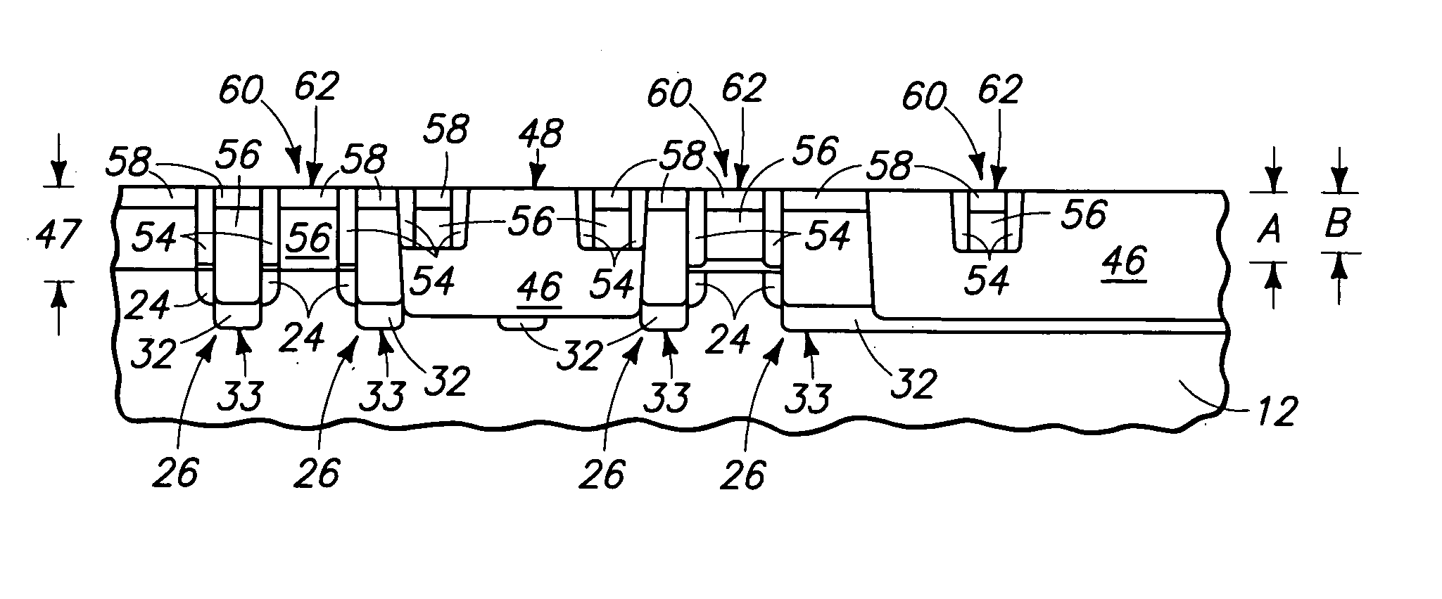
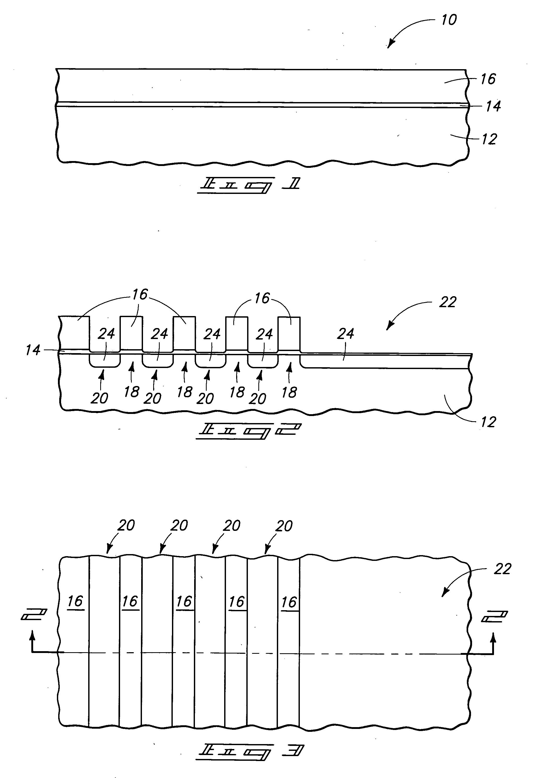
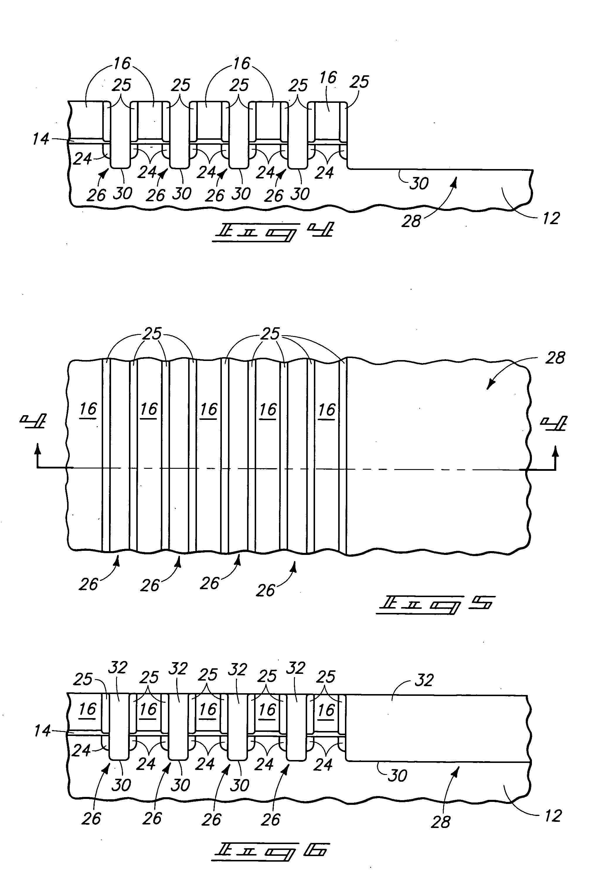
[0035] Preferred methods of forming field effect transistors are described with reference to FIGS. 1-20. FIG. 1 depicts a semiconductor substrate 10 comprising a bulk monocrystalline silicon substrate ˜12. In the context of this document, the term “semiconductor substrate” or “semiconductive substrate” is defined to mean any construction comprising semiconductive material, including, but not limited to, bulk semiconductive materials such as a semiconductive wafer (either alone or in assemblies comprising other materials thereon), and semiconductive material layers (either alone or in assemblies comprising other materials). The term “substrate” refers to any supporting structure, including, but not limited to, the semiconductive substrates described above. Also in the context of this doc...


PUM


Abstract

In one implementation, a method of forming a field effect transistor includes etching an opening into source / drain area of a semiconductor substrate. The opening has a base comprising semiconductive material. After the etching, insulative material is formed within the opening over the semiconductive material base. The insulative material less than completely fills the opening and has a substantially uniform thickness across the opening. Semiconductive source / drain material is formed within the opening over the insulative material within the opening. A transistor gate is provided operatively proximate the semiconductive source / drain material. Other aspects and implementations are contemplated.

Description

TECHNICAL FIELD [0001] This invention relates to methods of forming field effect transistors, and to methods of forming field effect transistor gates and gate lines. BACKGROUND OF THE INVENTION [0002] Semiconductor processors continue to strive to reduce the size of individual electronic components, thereby enabling smaller and denser integrated circuitry. One typical circuitry device is a field effect transistor. Typically, such includes opposing semiconductive source / drain regions of one conductivity type having a semiconductive channel region of opposite conductivity type therebetween. A gate construction is received over the channel region. Such includes a conductive region having a thin dielectric layer positioned between the conductive region and the channel region. Current can be caused to flow between the source / drain regions through the channel region by applying a suitable voltage to the gate. [0003] In some cases, the channel region is composed of a background doped semic...

Claims


Application Information

Patent Timeline
IPC IPC(8): G06K19/07H01L21/336H01L21/762H01L21/8234
CPCG06K19/0723H01L29/7833G06K19/07771H01L21/76229H01L21/76232H01L21/76264H01L21/823418H01L21/823437H01L21/823481H01L21/823814H01L21/823828H01L29/1083H01L29/41783H01L29/66545H01L29/66583H01L29/66628H01L29/66636H01L29/7834G06K19/0726
Inventor TANG, SANH D.VIOLETTE, MICHAEL P.BURKE, ROBERT
Owner MICRON TECH INC
Why Eureka
Try Eureka