Semiconductor manufacturing apparatus, semiconductor manufacturing method and wafer stage

a manufacturing apparatus and semiconductor technology, applied in the direction of semiconductor/solid-state device manufacturing, electric devices, basic electric elements, etc., can solve the problems of insufficient measurement of the temperature of the wafer at the time of the wafer processing, ineffective to the case, and insufficient wafer processing, so as to improve the quality of wafer processing on the wafer surfa

Inactive Publication Date: 2005-05-05
TRECENTI TECHNOLOGIES INC
View PDF0 Cites 48 Cited by
  • Summary
  • Abstract
  • Description
  • Claims
  • Application Information

AI Technical Summary

Benefits of technology

[0020] Namely, the equality in wafer proces

Problems solved by technology

Similarly, even if the configuration to independently change an electrostatic force between the center side and outer peripheral side of the surface is adopted, it is not effective to the case where the assumed inequality within the lone has been generated coaxially but not sufficient to the case where the inequality has been generated non-coaxially.
Further, in the wafer temperature control of the conventional method, no wafer temper

Method used


Image

  • Semiconductor manufacturing apparatus, semiconductor manufacturing method and wafer stage
  • Semiconductor manufacturing apparatus, semiconductor manufacturing method and wafer stage
  • Semiconductor manufacturing apparatus, semiconductor manufacturing method and wafer stage

Examples


first embodiment

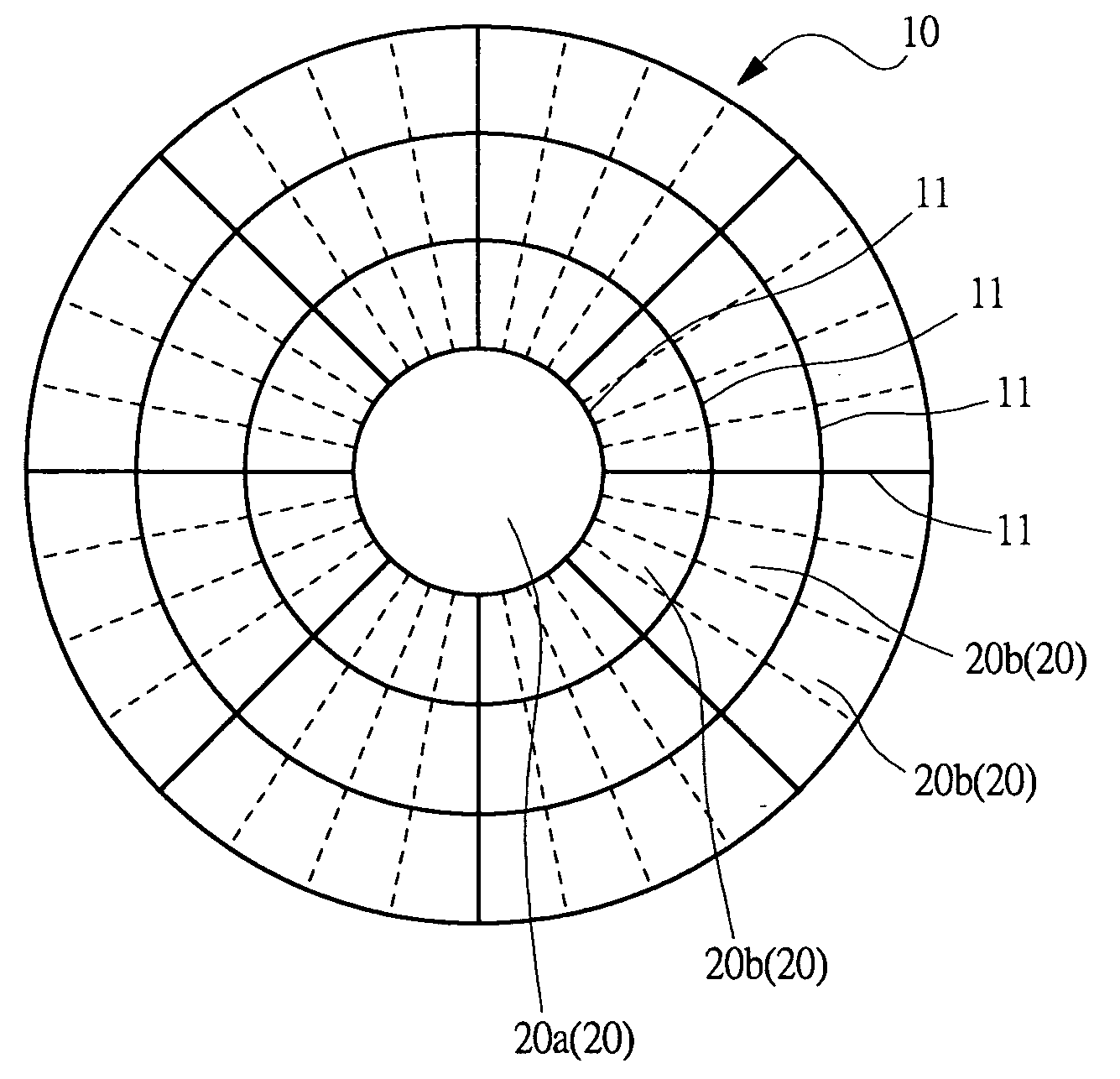
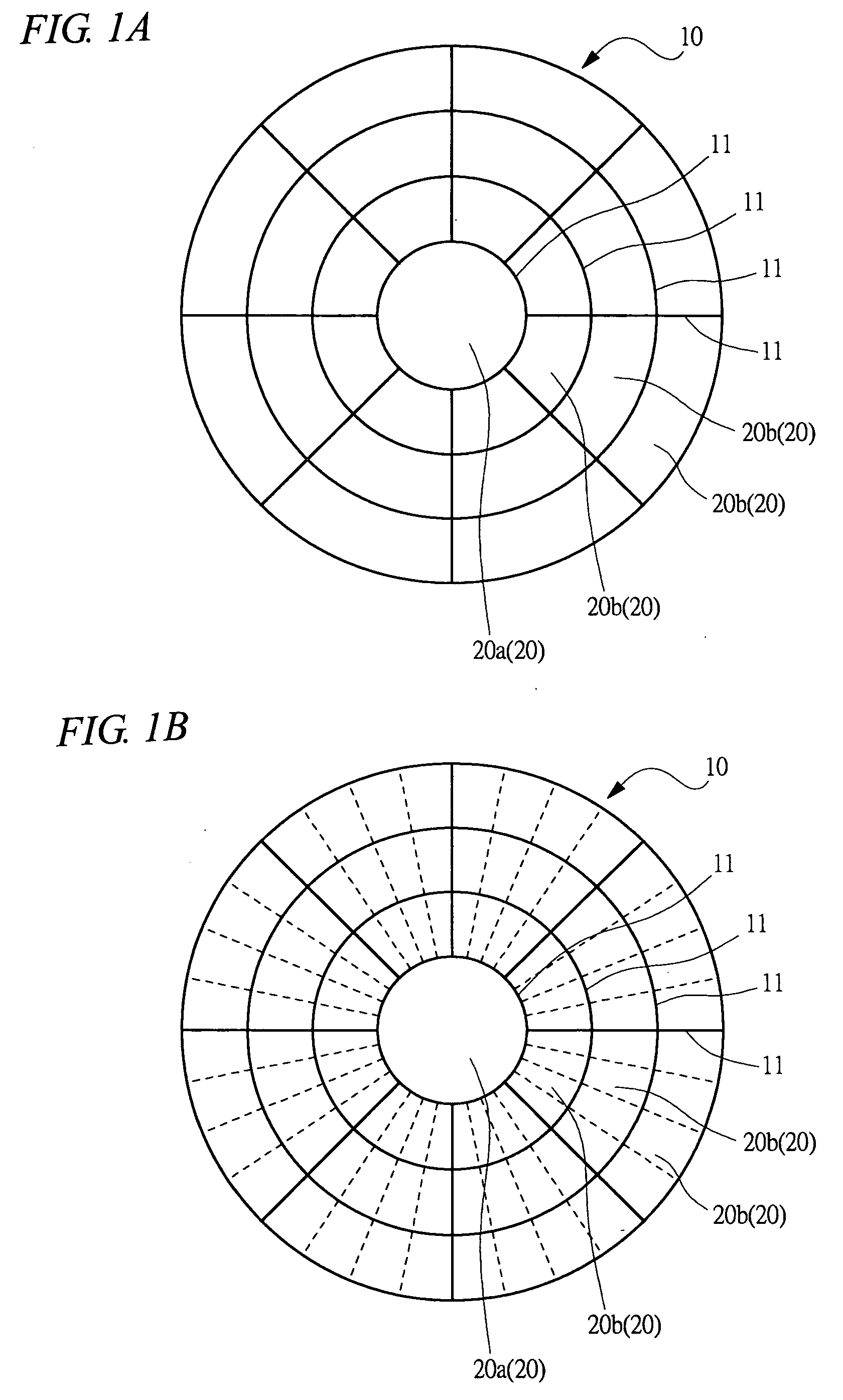
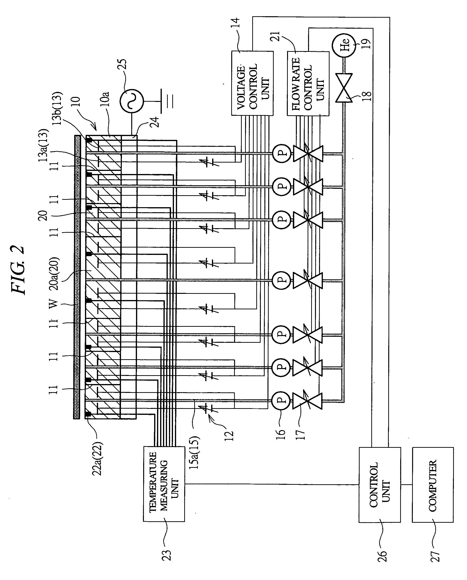
[0029] According to this embodiment, a wafer stage of the present invention will be described. FIG. 1A is a plan view showing schematically the condition of plural chucking areas on the wafer stage. FIG. 1B is an explanatory diagram showing schematically a condition in which the chucking area is further divided to smaller chucking areas. FIG. 2 is an explanatory diagram of the cross section showing schematically the structure of the wafer stage.

[0030] For this embodiment, a wafer stage employing electrostatic chucking force for use in a vacuum chamber for generating plasma such as a dry etching will be exemplified.

[0031] A wafer stage 10 has a stage main body 10a formed in a substantially fat circular disk of insulating material such as ceramic in order to hold a wafer W on its top face as shown in FIGS. 1A and 2.

[0032] As shown in FIG. 2, the stage main body 10a is divided into a plurality of sections by partition members 11 formed of insulating member. In FIG. 1A for example, t...

second embodiment

[0078] For this embodiment, an example in which a semiconductor device is manufactured using a dry etching unit having the wafer stage 10 described in the first embodiment will be described.

[0079] As the dry etching unit, for example, parallel flat plate type plasma etching unit can be assumed. As for the structure of that unit, the wafer stage 10 having the above-described structure for chucking a wafer electrostatically is provided within a vacuum chamber for generating plasma (not shown).

[0080] An upper electrode is provided in parallel to and opposing the lower electrode 24 on which the stage main body 10a of the wafer stage 10 is provided. Etching gas is supplied in between the upper electrode and the lower electrode and the supplied etching gas is formed to plasma between the upper and lower electrodes so as to dry-etch a wafer electrostatically chucked on the wafer stage 10.

[0081] In such a dry etching, inequality in processing accuracy within the wafer surface becomes pro...

third embodiment

[0104] For this embodiment, a method for solving the inequality in processing dimension within the surface accompanied by such dry etching by controlling the temperature within the surface of the wafer using the wafer stage 10 will be described. The inequality in processing accuracy within the wafer surface can be grasped as a difference in etching rate (difference in deposition amount for side wall protecting film) and such a difference in etching rate can be corrected by controlling the temperature within the wafer surface as described in the previous embodiment.

[0105] The wafer is processed with a dry etching apparatus having the above-described structure. From that processing result, a distribution of processing dimension within the surface is measured in step S210 as indicated in FIG. 5A. Consequently, assume that two areas, area A1 and area A2, exist separately as shown in FIG. 5B. Such a distribution of the processing dimension within the surface can be recognized through a ...


PUM


Abstract

A stage main body of a wafer stage having electrostatic chuck function is sectioned into plural chucking areas with partition members. Each chucking area includes electrodes capable of changing an applied voltage, a helium supply pipe and a fluorescent thermometer. The distribution of the temperature of a wafer is grasped at real time by measuring the temperature of the wafer corresponding to the plural chucking areas. A local temperature correction for the wafer is carried out by adjusting the electrostatic chucking force in the chucking area corresponding to a necessary temperature corrective area. By achieving the temperature control within the wafer surface in this way, the equality in wafer processing, which is affected by the wafer temperature, is secured thereby eliminating the inequality in processing accuracy of the wafer processing within a wafer surface.

Description

CROSS-REFERENCE TO RELATED APPLICATION [0001] The present application claims priority from Japanese Patent Application No. JP 2003-368402 filed on Oct. 29, 2003, the content of which is hereby incorporated by reference into this application. TECHNICAL FIELD OF THE INVENTION [0002] The present invention relates to an improvement technology for uniformity of a wafer surface upon manufacturing of a semiconductor device and more particularly to a technology which is effective when it is adopted for wafer processing in the conditions that the wafer is electrostatically chucked by a vacuum system. BACKGROUND OF THE INVENTION [0003] The technologies, which will be described, have been considered by the present inventor when the present invention is completed and the outline thereof will be explained briefly. When manufacturing a semiconductor device, various kinds of processings are carried out on a wafer, for example, a fine pattern lithography. At the time of this processing, the wafer i...

Claims


Application Information

Patent Timeline
IPC IPC(8): H01L21/3065H01L21/00H01L21/205H01L21/68H01L21/683
CPCH01L21/67109H01L21/6833H01L21/67248H01L21/68
Inventor USUAMI, HIROHISA
Owner TRECENTI TECHNOLOGIES INC
Why Eureka
Try Eureka