System for measuring periodic structures

a technology of periodic structure and metrology system, which is applied in the direction of optical radiation measurement, instruments, polarisation-affecting properties, etc., can solve the problems of large size and footprint compared to the wafer, cumbersome control of sizable apparatus, etc., and achieves the measurement of a single radiation parameter, reduce calculation time, and simple construction

Inactive Publication Date: 2005-05-12
ZHAO GUOHENG +3
View PDF15 Cites 9 Cited by
  • Summary
  • Abstract
  • Description
  • Claims
  • Application Information

AI Technical Summary

Benefits of technology

[0005] In many of the diffraction-based metrology or ellipsometric techniques for measuring the critical dimension, theoretical models employing libraries or non-linear regression are employed to find the critical dimension or other parameters of the periodic structure. Where the periodic structure measured is topographically complex, it may be necessary to measure more than one radiation parameter to get adequate information for the modeling process. Where the periodic st

Problems solved by technology

However, since the apparatus includes a number of components, it also has a significant size and footprint compared to that of the wafer.
F

Method used


Image

  • System for measuring periodic structures
  • System for measuring periodic structures
  • System for measuring periodic structures

Examples


Embodiment Construction

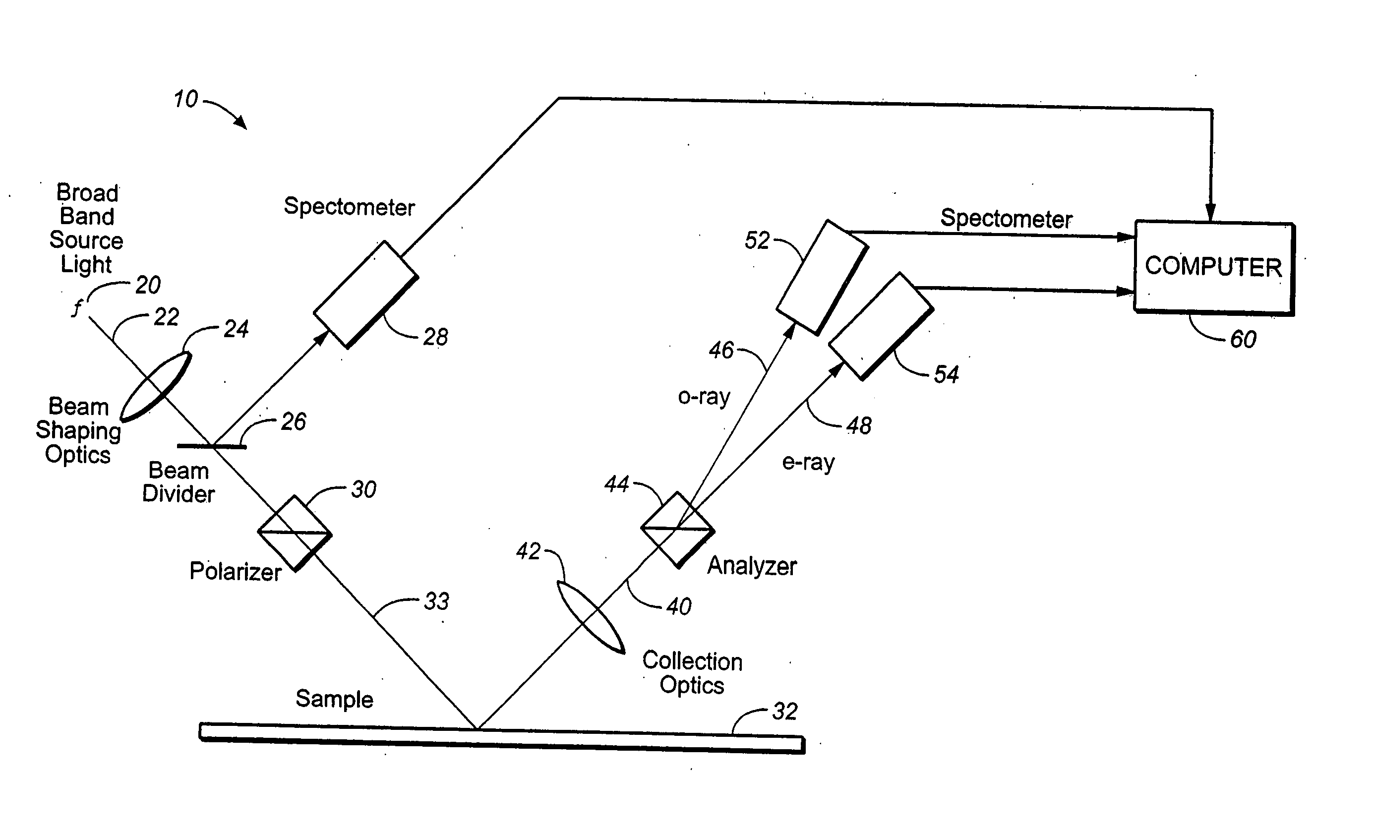
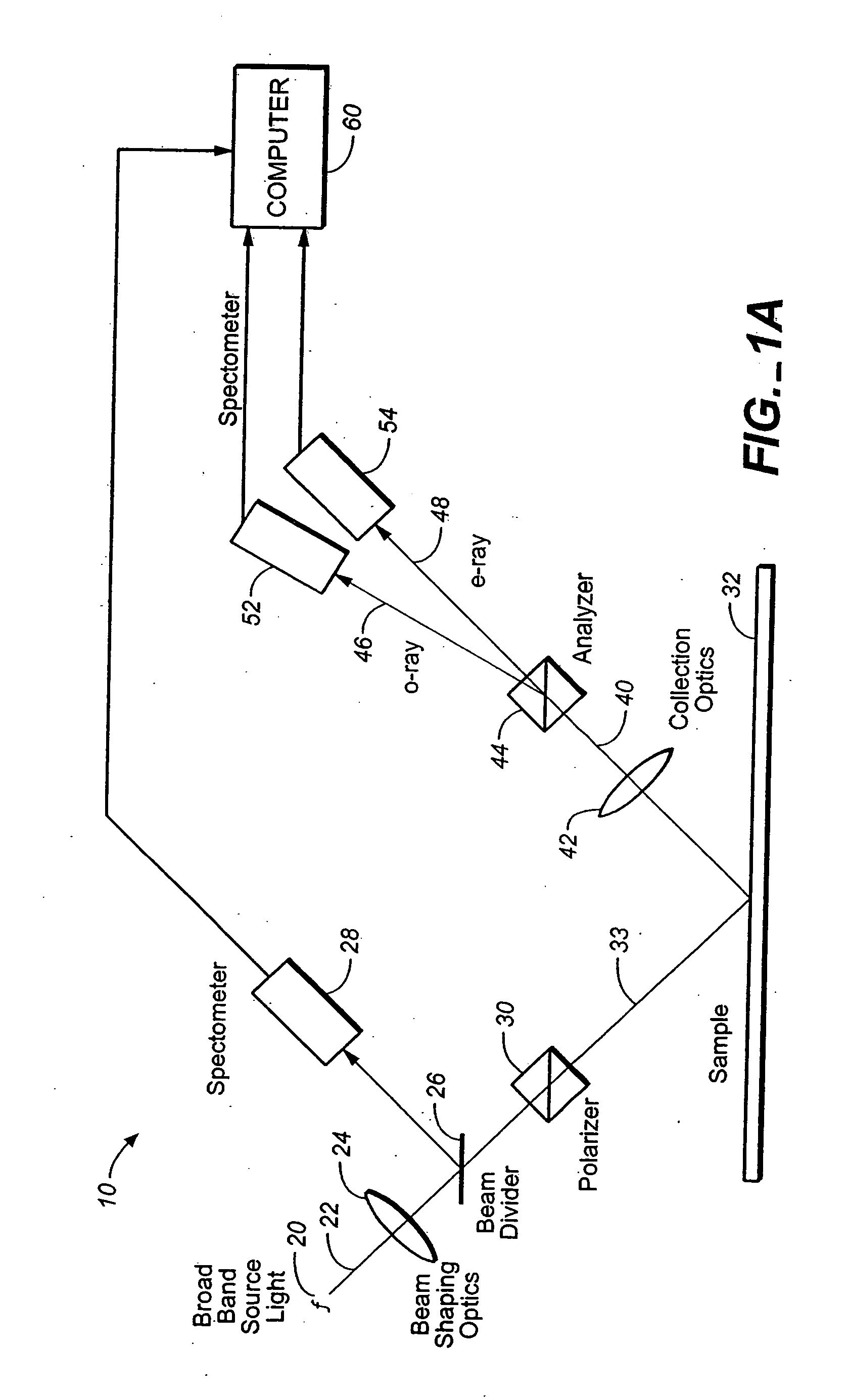
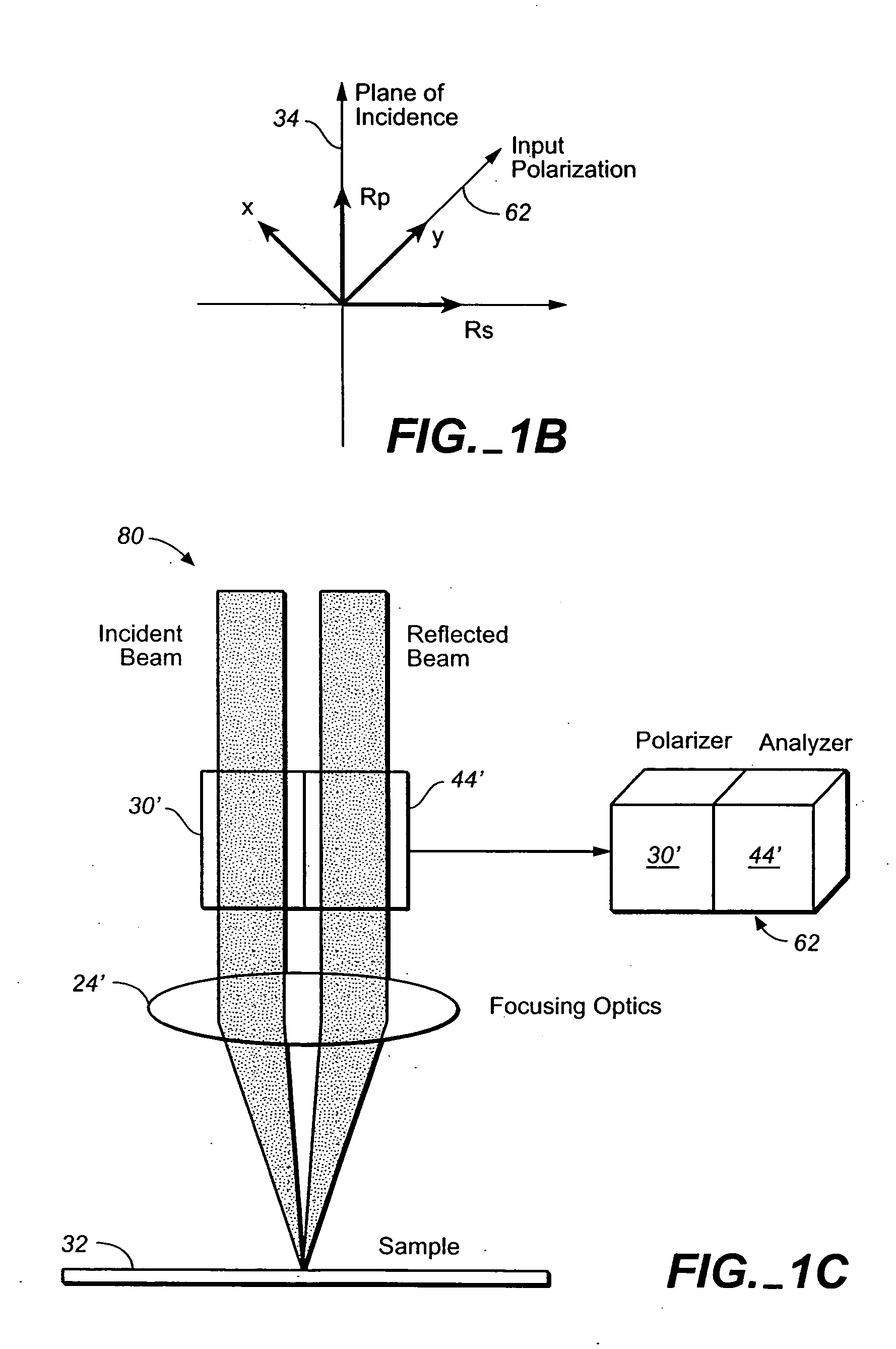
[0026] As shown in FIG. 1, a broadband source of electromagnetic radiation 20 provides a polychromatic beam with wavelength components preferably from 180 to 1000 nm. In one embodiment, source 20 may be a xenon lamp. The beam 22 from source 20 is shaped by beam shaping optics 24. A portion of the beam 22 is diverted by a beam divider 26 to spectrometer 28 for monitoring intensity variations in beam 22 in order to normalize the results of detection. Beam 22 is polarized by a polarizer 30 and the polarized beam is directed to sample 32 to illuminate a periodic structure thereon. Preferably the plane of incidence 34 (see FIG. 1B) of beam 22 is perpendicular to the grating lines in the periodic structure of sample 32. Radiation originating from beam 22 that has been modified by sample 32, such as by reflection or transmission, is collected by collection optics 42 as a collected beam 40 and passed through an analyzer 44 which splits the collected radiation into two rays: an extraordinary...


PUM


Abstract

A periodic structure is illuminated by polychromatic electromagnetic radiation. Radiation from the structure is collected and divided into two rays having different polarization states. The two rays are detected from which one or more parameters of the periodic structure may be derived. In another embodiment, when the periodic structure is illuminated by a poly chromatic electromagnetic radiation, the collected radiation from the structure is passed through a polarization element having a polarization plane. The element and the polychromatic beam are controlled so that the polarization plane of the element are at two or more different orientations with respect to the plane of incidence of the polychromatic beam. Radiation that has passed through the element is detected when the plane of polarization is at the two or more positions so that one or more parameters of the periodic structure may be derived from the detected signals. At least one of the orientations of the plane of polarization is substantially stationary when the detection takes place. To have as small a footprint as possible, one employs an optical device that includes a first element directing a polychromatic beam of electromagnetic radiation to the structure and a second optical element collecting radiation from the structure where the two elements form an integral unit or are attached together to form an integrated unit. To reduce the footprint, the measurement instrument and the wafer are both moved. In one embodiment, both the apparatus and the wafer undergo translational motion transverse to each other. In a different arrangement, one of the two motions is translational and the other is rotational. Any one of the above-described embodiments may be included in an integrated processing and detection apparatus which also includes a processing system processing the sample, where the processing system is responsive to the output of any one of the above embodiments for adjusting a processing parameter.

Description

BACKGROUND OF THE INVENTION [0001] This invention relates in general to optical techniques for measuring periodic structures, and in particular to an improved spectroscopic diffraction-based metrology system for measuring periodic structures, such as grating-type targets on semiconductor wafers. [0002] In conventional techniques, optical microscopes have been used for measuring the critical dimension (“CD”) for semiconductor lithographic processes. However, as the CD becomes smaller and smaller, it cannot be resolved at any practical available optical wavelengths in optical microscopy. Scanning electron microscope technology has extremely high resolution. However, this technology inherently requires large capital expenditures and heavy accessory equipment such as vacuum equipment, which makes it impractical for integration with lithographic processes. Two-theta-scatterometers face similar practical challenges for integration, as they require mechanical scanning over a wide range of ...

Claims


Application Information

Patent Timeline
IPC IPC(8): G01B11/00
CPCG01B11/00G01N21/956G01N21/4788G01N21/21
Inventor ZHAO, GUOHENGGROSS, KENNETH P.SMEDT, RODNEYNIKOONAHAD, MEHRDAD
Owner ZHAO GUOHENG
Why Eureka
Try Eureka