Semiconductor integrated circuit and data processing system

a technology of integrated circuits and data processing systems, applied in the direction of digital storage, memory adressing/allocation/relocation, instruments, etc., can solve the problem that two operations cannot be efficiently performed by using different memory banks, and achieve the effect of improving the speed of first access

Inactive Publication Date: 2005-05-12
RENESAS ELECTRONICS CORP
View PDF21 Cites 8 Cited by
  • Summary
  • Abstract
  • Description
  • Claims
  • Application Information

AI Technical Summary

Benefits of technology

[0009] A first object of the present invention is to enhance the speed of first access to a multi-bank memory, that is, the speed of read access different in word line from the previous access.
[0011] A third object of the present invention is to make non-blocking multi-access possible in a semiconductor integrated circuit having a plurality of multi-bank memory macro structures in which a plurality of access requests without conflict among the memory macro structures are allowed so that one access does not block another access.
[0012] A fourth object of the present invention is to enhance the efficiency of data rewrite to a multi-bank DRAM having a cache line with every word line. That is, the inventor has found that, when the cache line is provided as a rewrite unit, there is no necessity of performing read modify write to apply write data after storage information read out to a bit line by a word line selecting operation is latched by a sense amplifier, in the same manner as in a general DRAM.
[0015] A multi-bank memory macro structure is used and data are held in a sense amplifier in every memory bank. When access is hit to the data held in the sense amplifier, data latched by the sense amplifier are output so that the speed of first access to the memory macro structure can be made high. That is, every memory bank is made to function as a sense amplifier cache. To enhance the hit ratio of the sense amplifier cache (the ratio of hit on the data of the sense amplifier) more greatly, after access to one memory bank, the next address (obtained by addition of a predetermined offset) is self-prefetched so that data in the self-prefetching address is preread by a sense amplifier in another memory bank. The next address is used as a subject of self-prefetching on the basis of an empirical rule that CPU operation programs or a group of processing data are basically mapped on linear addresses.
[0020] Therefore, an address alignment control unit 41 is provided in the access controller for changing the bit alignment of an access address signal supplied from the outside to output the changed bit alignment to the memory macro structure. For example, the address alignment control unit is provided to allocate the alignment of an address signal supplied from the CPU and different from the alignment of a plurality of address bits allocated to the index address of the first level cache memory to the bank address of the memory bank. As a result, cache entry replacement caused by cache-miss of the first level cache memory can be performed without lowering of the operating efficiency of the multi-bank memory.
[0027] In a semiconductor integrated circuit in which a plurality of multi-bank memory macro structures are integrated, non-blocking multi-access can be provided for a plurality of access requests without conflict among memory macro structures so that one access does not block another access. The memory 6 for achieving this access comprises an access controller 4 having a first access port PT1 and a second access port PT2, and a plurality of memory macro structures 5Ma to 5Md connected to the access controller through data lines 9DBa to 9DBd respectively. Each of the memory macro structures has a plurality of memory banks BANK1 to BANK4 having bank addresses allocated thereto respectively. Each of the memory banks has a sense amplifier 53 for latching storage information read out to a bit line BL from a memory cell in a word line WL selected on the basis of a row address signal R-ADD. The bit line is selected on the basis of a column address signal C-ADD. The selected bit line is connected to a data line GBL of the memory macro structure. The access controller includes selectors 450R, 451R, 452W and 453W for selecting a memory macro structure accessed through the first access port and a memory macro structure accessed through the second access port, an access priority judgment unit 40 permitting parallel access through the two access ports when both the access through the first access port and access through the second access port use different memory macro structures respectively, an address / command generating unit 44 for generating the address / command and being able to operate for every memory bank in the memory macro structure to be accessed, and a hit / miss judgment unit 43 for making it possible to output data latched by the sense amplifier to the data line in response to an access request after the data latching.

Problems solved by technology

Accordingly, the two operations cannot be performed efficiently by use of different memory banks.

Method used


Image

  • Semiconductor integrated circuit and data processing system
  • Semiconductor integrated circuit and data processing system
  • Semiconductor integrated circuit and data processing system

Examples


Embodiment Construction

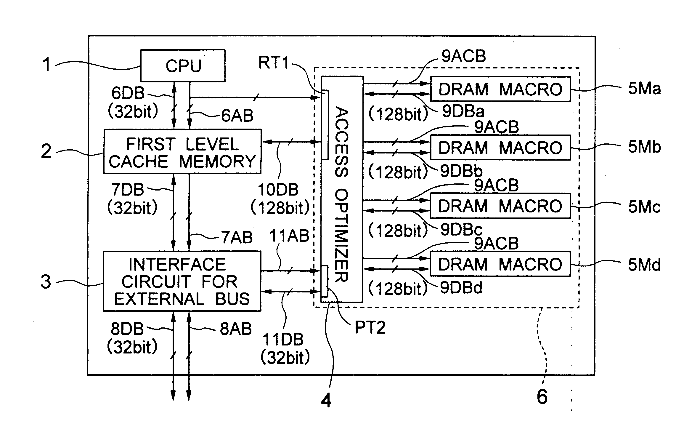
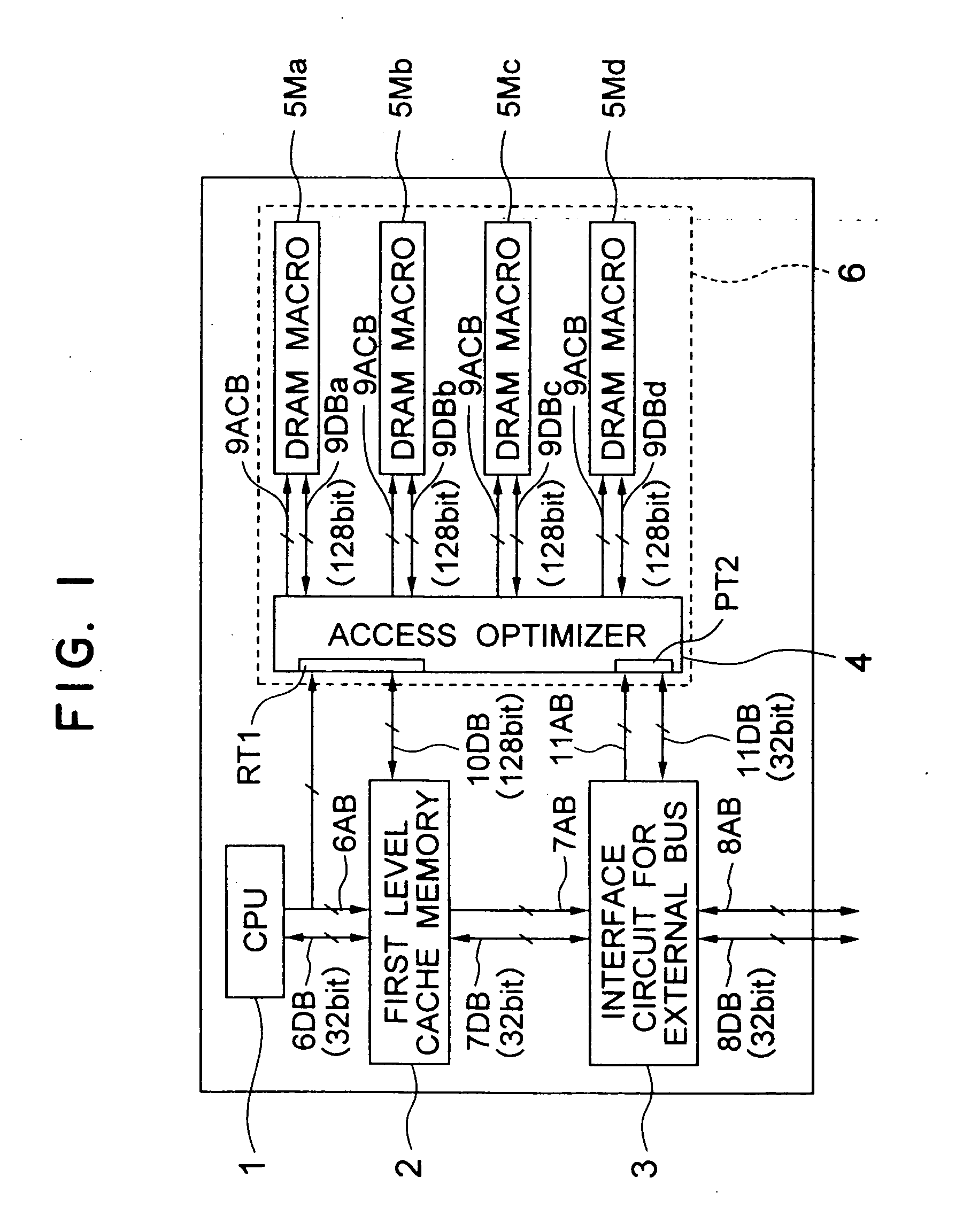
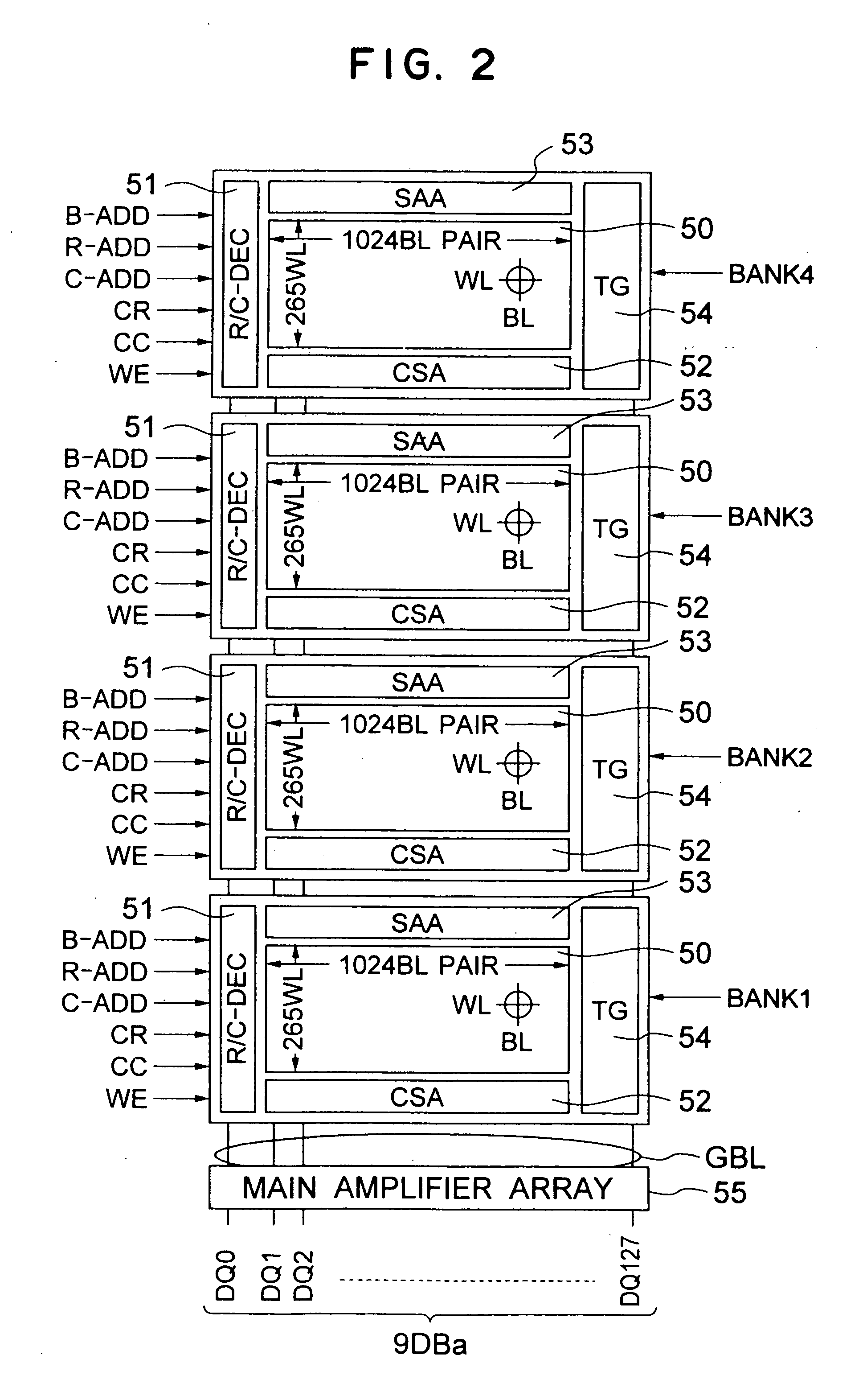
[0054]FIG. 1 shows an LSI integrating DRAM and CPU (referred to as system LSI) which is an example of a semiconductor integrated circuit according to the present invention. The system LSI shown in FIG. 1 is not limited specifically. A CPU 1 as an example of a large-scale logic circuit, a first level cache memory 2, an interface circuit 3 for external bus, an access optimizer 4 and a plurality of DRAM macro structures (multi-bank DRAMs) 5Ma to 5Md as an example of a large-capacity memory are integrated in one chip such as a monocrystalline silicon chip by a CMOS (Complementary Metal Oxide Semiconductor) producing technique. The DRAM macro structures 5Ma to 5Md are constituted by multi-bank DRAMs which have a plurality of DRAM banks (memory banks) respectively. The DRAM banks are provided with shared global bit lines. Each of the DRAM banks has a sense amplifier cache function using a sense amplifier as a cache. For access hit to data in the sense amplifier, data can be output at a hi...


PUM


Abstract

To enhance the speed of first access (read access different in word line from the previous access) to a multi-bank memory, multi-bank memory macro structures are used. Data are held in a sense amplifier for every memory bank. When access is hit to the held data, data latched by the sense amplifier are output to thereby enhance the speed of first access to the memory macro structures. Namely, each memory bank is made to function as a sense amplifier cache. To enhance the hit ratio of such a sense amplifier cache more greatly, an access controller self-prefetches the next address (an address to which a predetermined offset has been added) after access to a memory macro structure so that data in the self-prefetched address are preread by a sense amplifier in another memory bank.

Description

CROSS-REFERENCE TO RELATED APPLICATIONS [0001] The present invention is related to co-pending application Ser. No. 09 / 188,367 filed Nov. 10, 1998 and entitled “SEMICONDUCTOR IC DEVICE HAVING A MEMORY AND A LOGIC CIRCUIT IMPLEMENTED WITH A SINGLE CHIP”, which is incorporated in its entirety herein by reference. BACKGROUND OF THE INVENTION [0002] The present invention relates to a semiconductor integrated circuit in which memories are integrated. Particularly, it relates to a semiconductor integrated circuit in which a logic circuit such as a CPU (central processing unit) is integrated with a large-capacity memory in one chip. For example, it relates to a useful technique adapted for embedded DRAM which is integrated with a CPU and a first level cache memory in one and the same chip. [0003] Today, a semiconductor integrated circuit in which a large-scale logic circuit is integrated with a large-capacity memory in one chip is provided. In such a semiconductor integrated circuit, the nu...

Claims


Application Information

Patent Timeline
Patent Type & Authority Applications(United States)
IPC IPC(8): G06F12/08G11C7/06G11C7/10G11C11/401G11C11/4091G11C11/4093
CPCG06F12/0215G06F12/0893G06F13/161G06F2212/3042G11C2207/2245G11C7/1006G11C11/4091G11C11/4093G11C2207/104G11C7/065G06F12/08
Inventor AYUKAWA, KAZUSHIGEMIURA, SEIJISATOH, JUNWATANABE, TAKAOYANAGISAWA, KAZUMASAKANNO, YUSUKEMIZUNO, HIROYUKI
Owner RENESAS ELECTRONICS CORP
Why Eureka
Try Eureka