Check patentability & draft patents in minutes with Patsnap Eureka AI!

Flip-chip mounting circuit board, manufacturing method thereof and integrated circuit device

a technology of mounting circuit board and flip-chip, which is applied in the direction of electrical apparatus casing/cabinet/drawer, electrical device connection, and association of printed circuit non-printed electric components, etc., can solve the problems of destroying high mounting efficiency (yield) and product reliability, contact failure, and advancing further downsizing, and achieves high yield

Inactive Publication Date: 2005-05-19
TDK CORPARATION
View PDF4 Cites 89 Cited by
  • Summary
  • Abstract
  • Description
  • Claims
  • Application Information

AI Technical Summary

Benefits of technology

[0017] Another object of the present invention is to provide a flip-chip mounting circuit board which can prevent a short circuit between adjacent bumps and realize a desirable bump-electrode contact between the circuit board itself and an element mounted thereon, a manufacturing method of such a circuit board, and an integrated circuit device.

Problems solved by technology

In such a case, the conventional circuit boards shown in FIG. 5 to FIG. 7 have a problem in advancing further downsizing.
On the other hand, the structure shown in FIG. 7, in which the solder resist 116 is formed so as to almost entirely cover the conductor pattern 114, is likely to cause contact failures.
As described above, the conventional circuit boards easily cause short circuits or contact failures, which might ruin high mounting efficiency (yield) and product reliability.

Method used


Image

  • Flip-chip mounting circuit board, manufacturing method thereof and integrated circuit device
  • Flip-chip mounting circuit board, manufacturing method thereof and integrated circuit device
  • Flip-chip mounting circuit board, manufacturing method thereof and integrated circuit device

Examples


Embodiment Construction

[0039] A flip-chip mounting circuit board, a manufacturing method thereof, and an integrated circuit device according to an embodiment of the present invention will be explained in detail with respect to the drawings.

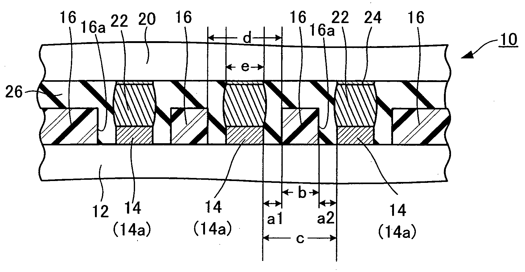
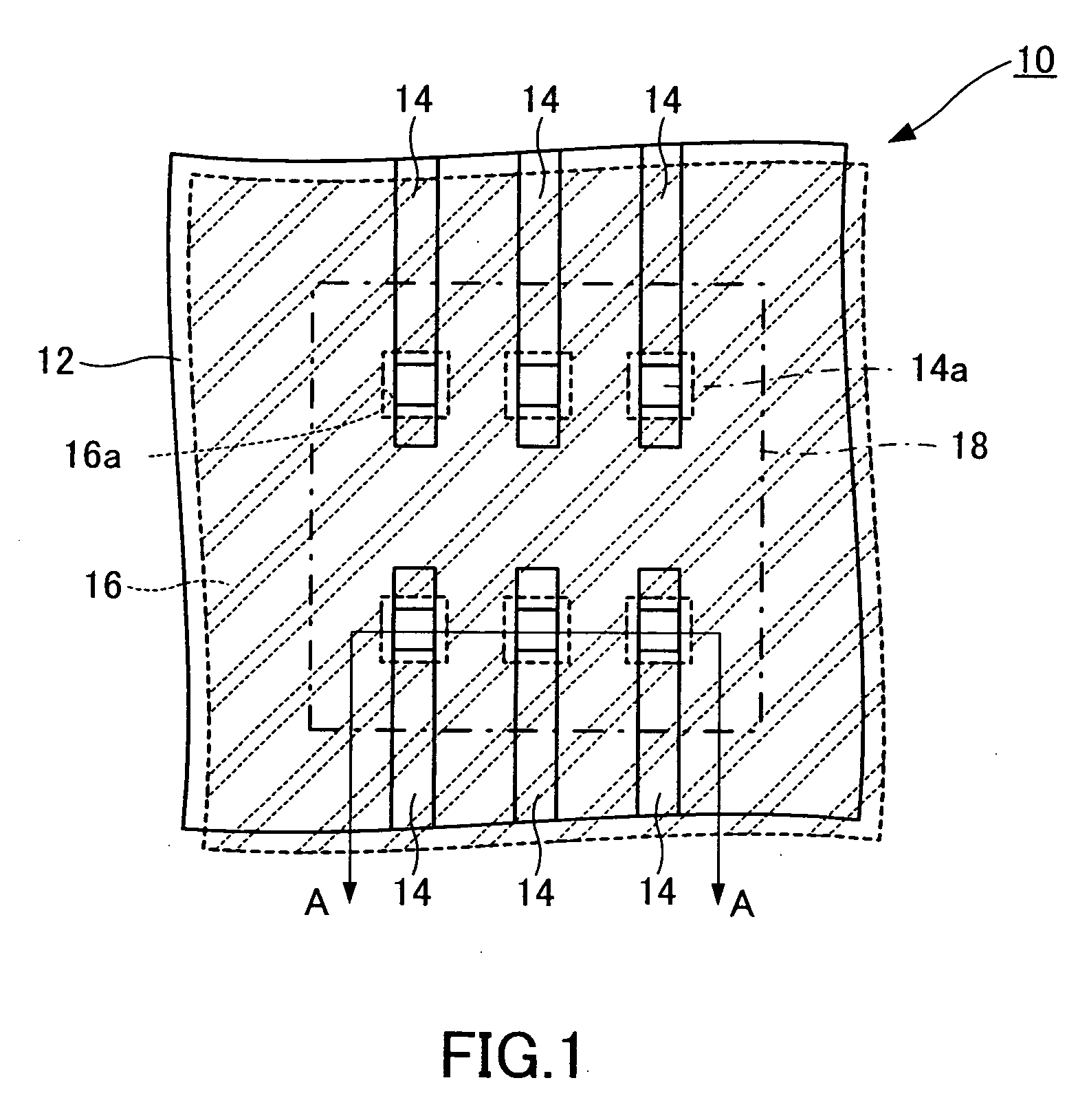
[0040]FIG. 1 shows an example of the structure of the flip-chip mounting circuit board 10 according to an embodiment of the present invention. In FIG. 1, for easier understanding, the region on which a semiconductor element chip 20 is to be mounted is illustrated as a mounting region 18 (the region indicated by a chain line in FIG. 1). Further, in FIG. 1, for easier understanding, the end of a solder resist 16 and the end of a board 12 are deviated. However, the solder resist 16 is actually formed on almost the entire surface of the board 12.

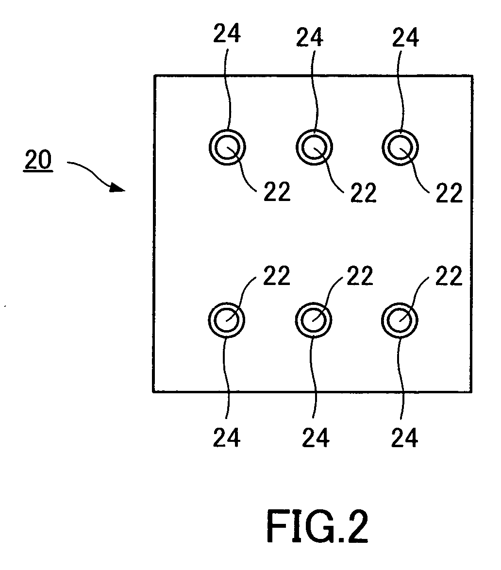
[0041] A flip-chip mounted circuit is a circuit obtained by mounting the semiconductor element chip 20 on the flip-chip mounting circuit board 10. An integrated circuit device is a device having this flip-chip mounted circuit.

[00...


PUM


Abstract

A conductor pattern having joint portions to which electrodes of a semiconductor element chip are to be joined is formed on a board on which the semiconductor element chip is to be mounted. Further, a solder resist is formed on the board so as to be apart from both of adjacent joint portions by a predetermined distance and so as to space the adjacent joint portions from each other.

Description

CROSS REFERENCE TO RELATED APPLICATION [0001] This application claims priority to Japanese Patent Application No. 2003-341309 filed on Sep. 30, 2003, and is incorporated herein by reference. BACKGROUND OF THE INVENTION [0002] 1. Field of the Invention [0003] The present invention relates to a flip-chip mounting circuit board for mounting a semiconductor element chip thereon, a manufacturing method thereof, and an integrated circuit device. [0004] 2. Description of the Related Art [0005] Recently, along with a request for downsizing electronic apparatuses, high-density packaging of circuit modules is demanded. For this demand, circuit boards are changed from both-surface wiring types to multilevel interconnection types and active elements are increasingly miniaturized. Further, semiconductor devices are changed from plastic mold semiconductors to bare chip semiconductors, and flip-chip mounting is developed as one of bare-chip mounting methods as disclosed in the Unexamined Japanese ...

Claims


Application Information

Patent Timeline
IPC IPC(8): H01L21/60H01L21/56H01L23/12H01L23/498H01R13/52H05K1/18H05K3/34H05K5/00
CPCH01L21/563H01L2224/16237H01L23/49894H01L2224/73203H01L2924/01078H01L2924/01079H01R13/5216H05K3/3452H05K2201/0989H05K2201/10674H05K2201/10977H01R12/52H01L2224/16225H01L2224/16238H01L2224/32225H01L2224/73204H01L2224/81191H01L23/49816H01L2924/00H01L24/05H01L2224/05568H01L2224/05573H01L2224/05624H01L2224/0615H01L2924/00014
Inventor KANEYUKI, TOMOHIKO
Owner TDK CORPARATION
Features
  • R&D
  • Intellectual Property
  • Life Sciences
  • Materials
  • Tech Scout
  • Unparalleled Data Quality
  • Higher Quality Content
  • 60% Fewer Hallucinations
Learn More