Signal level detector and amplification factor control system using signal level detector

a technology of signal level detector and control system, applied in the direction of pulse manipulation, pulse technique, multi-input and output pulse circuit, etc., can solve the problem of inability to perform stable detection

Inactive Publication Date: 2005-05-19
KK TOSHIBA
View PDF13 Cites 36 Cited by
  • Summary
  • Abstract
  • Description
  • Claims
  • Application Information

AI Technical Summary

Benefits of technology

[0036]FIG. 9 is a waveform diagram illustrating an operation within an operation range of an amplification factor control system according to the present invention;
[0037]FIG. 10 is a waveform diagram illustrating an operation out of the operation range of the amplification factor control system according to the present invention (when an input power

Problems solved by technology

The detector simply using a squaring circuit in this manner has a problem that the stable detection cannot be performed because the detector includes the circuit/

Method used


Image

  • Signal level detector and amplification factor control system using signal level detector
  • Signal level detector and amplification factor control system using signal level detector
  • Signal level detector and amplification factor control system using signal level detector

Examples


first embodiment

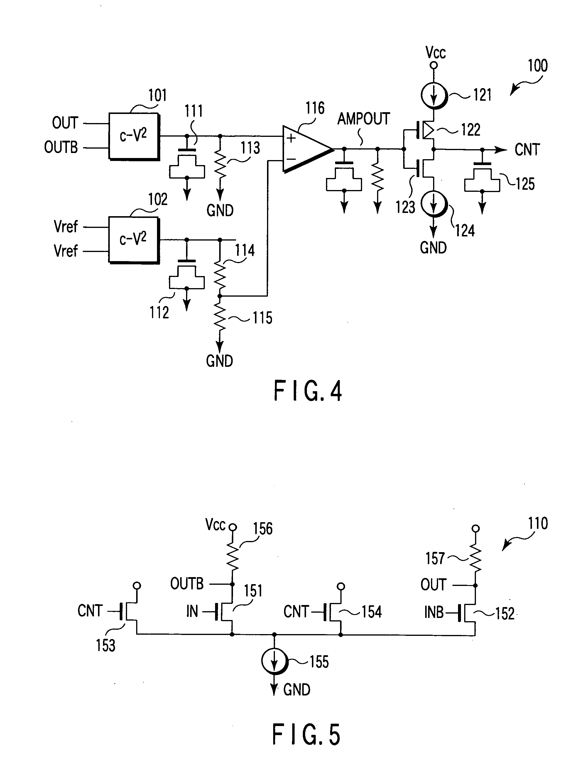
[0054]FIG. 4 shows a signal level detection according to the first embodiment of the present invention. Differential signals OUT and OUTB are inputted to a first squaring circuit 101, and an output from this circuit is inputted to one input terminal of a differential amplifier 116 as a comparison circuit. A capacitance element 111 and a resistor 113 are connected between an output terminal of the first squaring circuit 101 and a ground terminal (GND). The capacitance element 111 is inserted in order to filter a second harmonic component in an input signal.

[0055] The same reference voltages Vref are inputted to two input terminals of a second squaring circuit 102, an output current from this circuit is converted into a voltage by resistance elements 114 and 115, and a divided voltage is inputted to the other input terminal of the differential amplifier 116. A capacitance element 112 is also connected between an output terminal of the second squaring circuit 101 and the ground in ord...

second embodiment

[0083]FIG. 13 shows a signal level detector according to a second embodiment of the present invention. In order to facilitate understanding, like reference numerals denote parts equal to those in the first embodiment. Differential signals OUT and OUTB are inputted to a first squaring circuit 101b, and different reference voltages Vref1 and Vref2 are inputted to two input terminals of a second squaring circuit 102b. Output terminals of the first and second squaring circuits are directly connected to each other, and a capacitance element 111 is connected between the output terminal of these circuits and GND. The capacitance element 111 is inserted in order to filter a double harmonic component in an input signal.

[0084] A total output from the first and second squaring circuits is inputted to a common gate of an output stage that a p channel side constant current source 121, a p channel transistor 122, an n channel transistor 123 and an n channel side constant current source 124 are c...

third embodiment

[0098]FIG. 18 shows a signal level detector according to the third embodiment of the present invention. Like reference numerals denote parts equal to those in the first and second embodiments, thereby eliminating tautological explanation. Since a second squaring circuit 102 outputs a voltage Vout2=Itail=bdVref2 which depends on a difference dVref between two reference voltages Vref1 and Vref2, the logic of AMPOUT is reversed when Vout1=Vout2, i.e., vpp=dVref is established. Therefore, the same advantages as those in the second embodiment can be obtained. It is to be noted that the circuit depicted in FIG. 5 can be used for the AMP 110 used to form an amplification factor control system.

[0099] In the circuit configuration shown in FIG. 18, a control signal CNT is also increased as an output voltage OUT of the AMP 110 is increased. The third embodiment is not restricted to such a circuit configuration, and it may have a circuit configuration that the control voltage CNT is decreased ...


PUM


Abstract

A signal level detector comprises a first voltage/current conversion circuit which outputs a first current which depends on a voltage amplitude of an inputted signal, a second voltage/current conversion circuit which outputs a second current which depends on an inputted reference voltage signal, and a comparison circuit which compares the first current with the second current and outputs an output current based on a comparison result.

Description

CROSS-REFERENCE TO RELATED APPLICATIONS [0001] This application is based upon and claims the benefit of priority from the prior Japanese Patent Application No. 2003-388077, filed Nov. 18, 2003, the entire contents of which are incorporated herein by reference. BACKGROUND OF THE INVENTION [0002] 1. Field of the Invention [0003] The present invention relates to a signal level detector for use in a wireless communication integrated circuit system and an amplification factor control system using this signal level detector. For example, the present invention relates to a signal level detector using a circuit which outputs a current which depends on an input voltage amplitude, and an amplification factor control system using this signal level detector. [0004] 2. Description of the Related Art [0005] Although an integrated circuit device is in heavy usage in wireless communication, FIG. 1 shows a block diagram of a Bluetooth LSI (15) used in a transceiver system as an example. The LSI 15 i...

Claims


Application Information

Patent Timeline
IPC IPC(8): H03G3/20H03D1/18H03G3/30H03K5/08H03K5/22H03K5/24H03K5/26
CPCH03K5/082H03K5/26H03K5/2481
Inventor TANZAWA, TORUHAMADA, MOTOTSUGU
Owner KK TOSHIBA
Why Eureka
Try Eureka