Integration of ALD tantalum nitride for copper metallization

a technology of ald tantalum nitride and copper metallization, which is applied in the direction of coating, chemical vapor deposition coating, coating process of metallic materials, etc., can solve the problems of reducing the reliability of the overall circuit, and reducing the diffusion rate of copper

Inactive Publication Date: 2005-05-19
APPLIED MATERIALS INC
View PDF99 Cites 191 Cited by
  • Summary
  • Abstract
  • Description
  • Claims
  • Application Information

AI Technical Summary

Problems solved by technology

However, copper diffuses more readily into surrounding materials and can alter the electronic device characteristics of the adjacent layers.
The diffused copper can form a conductive path between layers thereby reducing the reliability of the overall circuit and may even result in device failure.

Method used


Image

  • Integration of ALD tantalum nitride for copper metallization
  • Integration of ALD tantalum nitride for copper metallization
  • Integration of ALD tantalum nitride for copper metallization

Examples


Embodiment Construction

Barrier Deposition Process

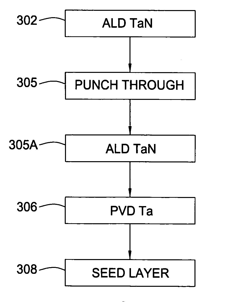
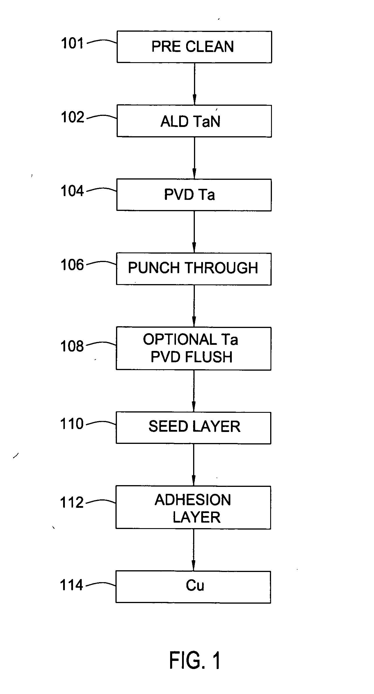
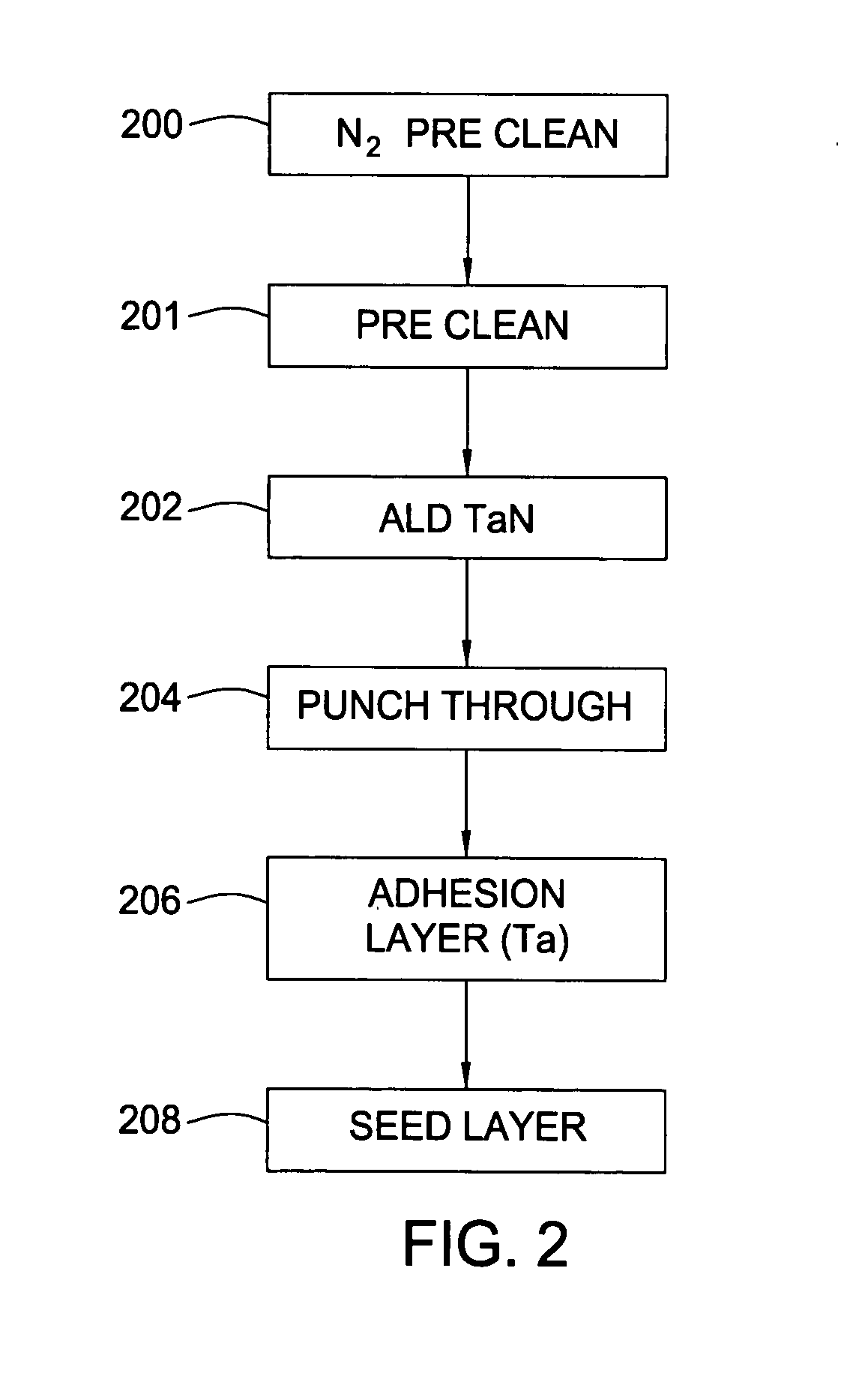
[0026]FIG. 1 illustrates one embodiment of a process of utilizing ALD tantalum nitride deposition in the formation of metal interconnect structures. In step 101, preconditioning occurs to prepare the surface for additional modification. The preconditioning options include nitrogen plasma, water plasma, hydrogen and helium plasma, low energy plasma, pre-flash with titanium or aluminum, or other precleaning process. In step 102, tantalum nitride is deposited by atomic layer deposition over a substrate structure. In step 104, a tantalum layer is deposited by physical vapor deposition over the tantalum nitride formed in step 102. In step 106, a punch-through step is performed to remove a portion of the tantalum nitride deposited in step 102 and to remove a portion of the tantalum deposited in step 104. In step 108, an optional titanium flash step may be performed to deposit tantalum by physical vapor deposition over the resulting substrate structure of step 1...


PUM

PropertyMeasurementUnit
temperatureaaaaaaaaaa
pressureaaaaaaaaaa

Abstract

A method and apparatus for depositing a tantalum nitride barrier layer is provided for use in an integrated processing tool. The tantalum nitride is deposited by atomic layer deposition. The tantalum nitride is removed from the bottom of features in dielectric layers to reveal the conductive material under the deposited tantalum nitride. Optionally, a tantalum layer may be deposited by physical vapor deposition after the tantalum nitride deposition. Optionally, the tantalum nitride deposition and the tantalum deposition may occur in the same processing chamber.

Description

CROSS-REFERENCE TO RELATED APPLICATIONS [0001] This application claims benefit of U.S. Provisional Patent application Ser. No. 60 / 478,663, filed Jun. 13, 2003, and titled, “Integration of ALD Tantalum Nitride for Copper Metallization.” This application is a continuation in part of U.S. patent application Ser. No. 10 / 193,333, filed Jul. 10, 2002, which claims the benefit of U.S. Provisional Patent Application Ser. No. 60 / 346,086, filed on Oct. 26, 2001, and is a continuation-in-part of U.S. patent application Ser. No. 09 / 965,370, filed on Sep. 26, 2001, U.S. patent application Ser. No. 09 / 965,373, filed on Sep. 26, 2001 and U.S. patent application Ser. No. 09 / 965,369, filed on Sep. 26, 2001, which are incorporated by reference herein.BACKGROUND OF THE INVENTION [0002] 1. Field of the Invention [0003] Embodiments of the present invention relate to a method for manufacturing integrated circuit devices. More particularly, embodiments of the invention relate to a system and process of ut...

Claims


Application Information

Patent Timeline
Patent Type & Authority Applications(United States)
IPC IPC(8): H01L21/44
CPCC23C16/34H01L21/76871C23C16/45504C23C16/45508C23C16/45512C23C16/45525C23C16/45544C23C16/45563C23C16/45582H01L21/02063H01L21/28562H01L21/76805H01L21/76843H01L21/76844H01L21/76846H01L21/76862H01L21/76865C23C16/4411
Inventor CHUNG, HUAMAITY, NIRMALYAYU, JICKMOSELY, RODERICK CRAIGCHANG, MEI
Owner APPLIED MATERIALS INC
Why Eureka
Try Eureka