Copper CMP defect reduction by extra slurry polish

a technology of slurry polish and copper, which is applied in the direction of semiconductor/solid-state device manufacturing, basic electric elements, electric apparatus, etc., can solve the problems of difficult removal from the surface of a charged layer, inability to rinse as in steps c and d, and reduce the number of particle defects produced, reduce the down force of the polishing pad during di water rinse segments of the oxide polish process, and reduce the defect number

Inactive Publication Date: 2005-05-19
TAIWAN SEMICON MFG CO LTD
View PDF6 Cites 35 Cited by
  • Summary
  • Abstract
  • Description
  • Claims
  • Application Information

AI Technical Summary

Benefits of technology

[0010] An objective of the present invention is to reduce the number of particle defects on a substrate following an oxide buffing process.
[0014] At this point, a first copper polish step is performed on a first platen in a CMP tool that lowers the level of the copper layer until it is approximately coplanar with the diffusion barrier layer. A second polish step on a second platen is used to remove the diffusion barrier layer above the dielectric layer. A third polish step is performed on a third platen in the CMP tool and involves an oxide polish process where a first oxide slurry application is followed by a DI water rinse and then a second application of the oxide slurry is followed by a second DI water rinse. The oxide polish process is optimized so that the total time for all steps remains unchanged from a prior art method with only one oxide slurry application. Therefore, throughput is not affected. The down force of the polishing pad during DI water rinse segments of the oxide polish process is lowered compared to a prior art method and this adjustment also helps to reduce the number of particle defects produced during the oxide polish process.
[0015] In one embodiment, each step of the oxide polish process is run for a fixed period of time that does not vary from wafer to wafer as in a lot based method. In a second embodiment, the oxide polish process may be integrated with an advanced process control (APC) system that is wafer based and has feed forward and feed backward components for adjusting the polish time for each wafer on a real time basis. A wafer based APC system is able to compensate for process variations and thereby maintain sheet resistance (Rs) values for the resulting copper interconnects within specified limits.

Problems solved by technology

Further water rinsing as in steps C and D may not be able to dislodge particle 30 and it remains as a defect in the prior art method.
The passivating agent is generally a polar compound and may be difficult to remove from the surface of a charged layer.

Method used


Image

  • Copper CMP defect reduction by extra slurry polish
  • Copper CMP defect reduction by extra slurry polish
  • Copper CMP defect reduction by extra slurry polish

Examples


Embodiment Construction

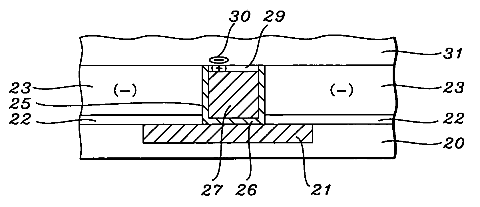
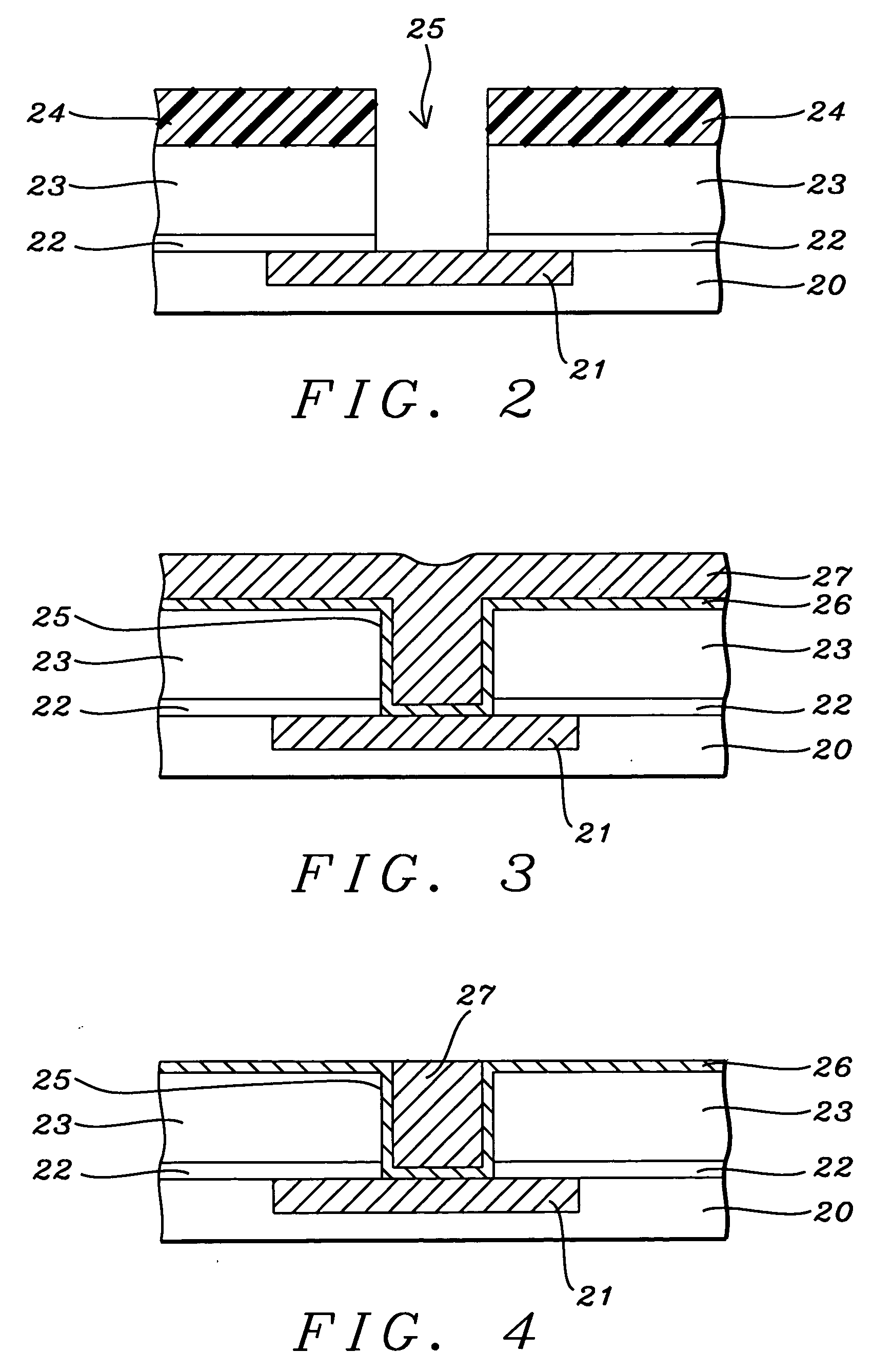
[0022] The present invention is especially useful in reducing the amount of particle defects formed as the result of a CMP process flow in a damascene scheme that includes three different polish processes at three different polish stations. In one embodiment, the present invention is an oxide polish process that follows a first CMP process in which a copper layer is substantially planarized and a second CMP process where a diffusion barrier layer is removed from the surface of a dielectric layer. Although the drawings depict the application of the CMP process flow to the fabrication of a copper interconnect formed in a via above an underlying metal layer, the drawings are not intended to limit the scope of the invention and other applications are possible. For example, the interconnect may also be a contact to an underlying conductive layer such as a source / drain region in a transistor. Optionally, the copper interconnect fills a trench and an underlying via in a dual damascene stru...


PUM

PropertyMeasurementUnit
temperatureaaaaaaaaaa
flow rateaaaaaaaaaa
water flow rateaaaaaaaaaa

Abstract

An oxide polishing process that is part of a CMP process flow is disclosed. After a copper layer is polished at a first polishing station and a diffusion barrier layer is polished at a second polishing station, a key sequence at a third polish station is the application of a first oxide slurry and a first DI water rinse followed by a second oxide slurry and then a second DI water rinse. As a result, defect counts are reduced from several thousand to less than 100. Another important factor is a low down force that enables more efficient particle removal. The improved oxide polishing process has the same throughput as a single oxide polish and a DI water rinse method and may be implemented in any three slurry copper CMP process flow.

Description

RELATED PATENT APPLICATION [0001] This application is related to attorney docket number TS02-992, Ser. No. ______, filing date ______, and to attorney docket number TS03-424, Ser. No. 10 / 627,795, filing date Jul. 25, 2003; assigned to a common assignee.FIELD OF THE INVENTION [0002] The invention relates to the field of fabricating high speed integrated circuits and in particular to a method of reducing the number of defects on a substrate following a chemical mechanical polishing (CMP) step of a copper interconnect structure. BACKGROUND OF THE INVENTION [0003] The use of copper wiring as interconnects in semiconductor devices has increased dramatically as ground rules shrink in order to reduce resistivity in the metal wiring. Interconnects are typically formed by a damascene approach in which a metal is deposited in an opening etched into one or more dielectric layers on a substrate. Although copper has a lower resistivity than Al or W, copper has a higher tendency to migrate into a...

Claims


Application Information

Patent Timeline
Patent Type & Authority Applications(United States)
IPC IPC(8): B24B1/00H01L21/02H01L21/302H01L21/3105H01L21/321H01L21/461H01L21/4763H01L21/768
CPCH01L21/02065H01L21/02074H01L21/7684H01L21/3212H01L21/31053
Inventor HONG, WILLIAMCHUANG, CHIA-CHECHUNG, CHI-WEICHIOU, WEN-CHIHCHEN, YING-HOJANG, SYUN-MING
Owner TAIWAN SEMICON MFG CO LTD
Why Eureka
Try Eureka