Nitride semiconductor substrate, method of fabrication thereof, and semiconductor element built thereon

a technology of nitride semiconductor and semiconductor layer, which is applied in the direction of basic electric elements, electrical equipment, semiconductor devices, etc., can solve the problems of inconvenient linear expansion coefficient, inability to completely satisfy silicon as a substrate material, and easy stress of nitride semiconductor layer or layer, so as to reduce the amount of leakage current flowing and low resistance

Active Publication Date: 2005-05-26
SANKEN ELECTRIC CO LTD
View PDF10 Cites 63 Cited by
  • Summary
  • Abstract
  • Description
  • Claims
  • Application Information

AI Technical Summary

Benefits of technology

[0009] The present invention seeks, in the substrate system of the kind under consideration, to prevent the buffer region, which is interposed between the substra

Problems solved by technology

Silicon is not, however, wholly satisfactory as a substrate material: There is an inconveniently great difference in linear expansion coefficient between the silicon substrate proper and the nitride semiconductor layer or layers.
The nitride semiconductor layer or layers had been easy to be stressed as a result, with the consequent development of cracks and transitions.
Thus the prior art multilayered buffer region provided a path of leakage current for the semico

Method used


Image

  • Nitride semiconductor substrate, method of fabrication thereof, and semiconductor element built thereon
  • Nitride semiconductor substrate, method of fabrication thereof, and semiconductor element built thereon
  • Nitride semiconductor substrate, method of fabrication thereof, and semiconductor element built thereon

Examples


embodiment

of FIG. 8

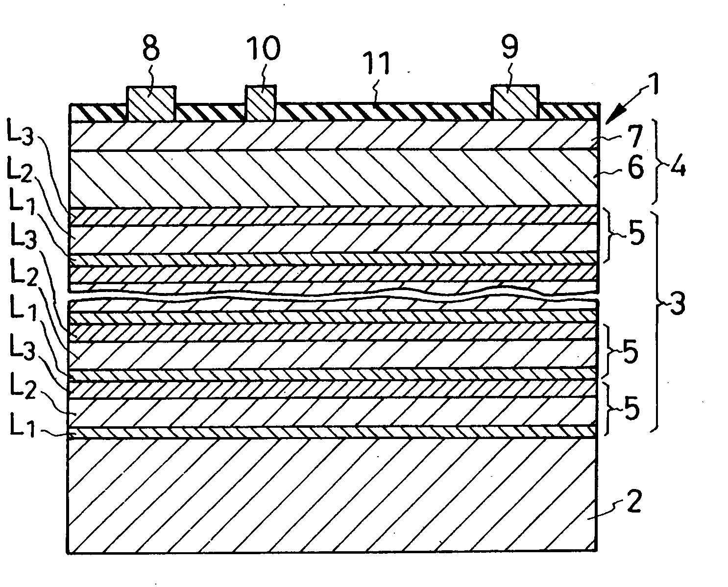
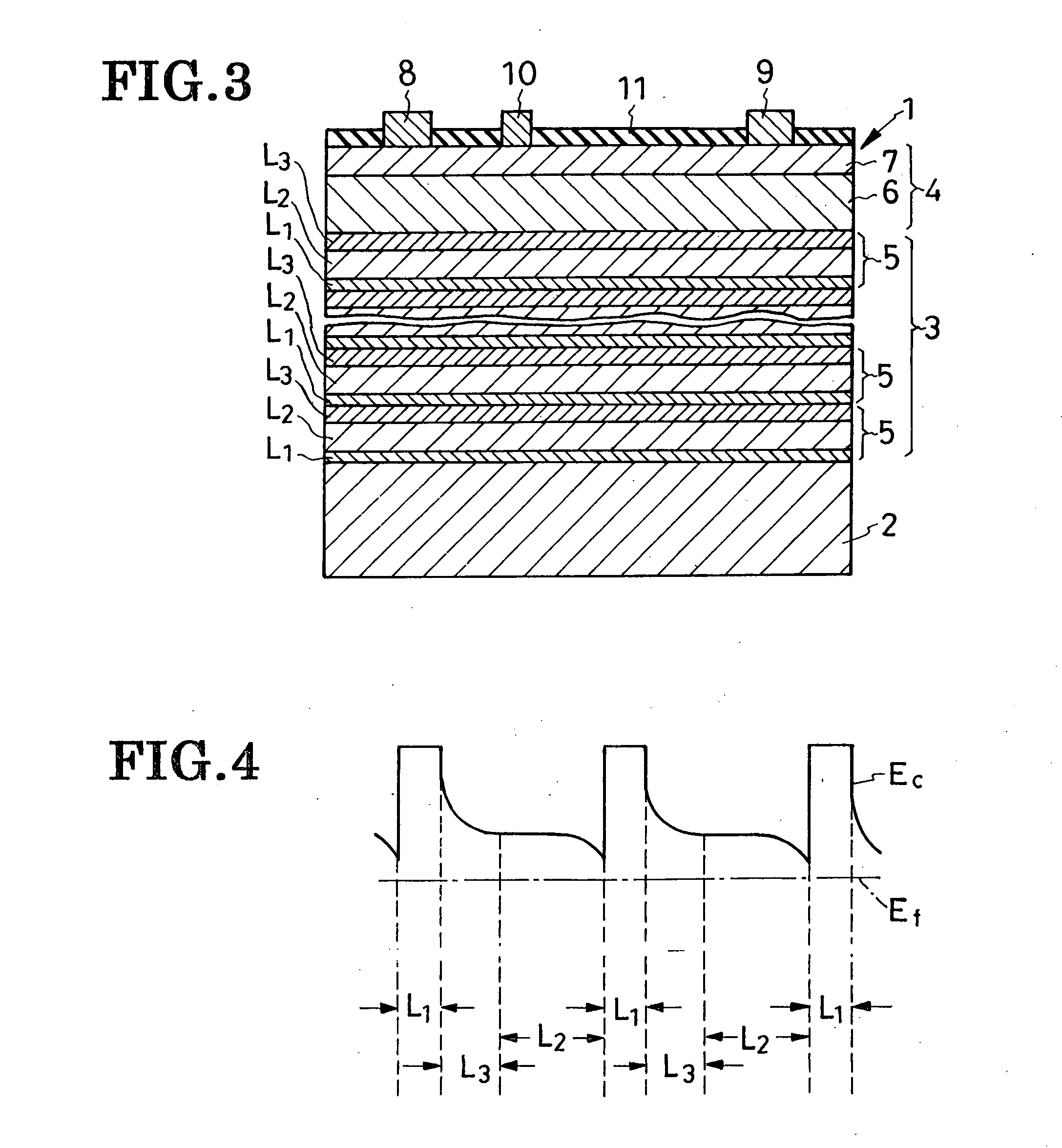
[0080] In FIG. 8 is shown still another substrate system 1b which is akin to the FIG. 3 substrate system 1 except for a main semiconductor region 4a. Unlike the main semiconductor region 4 for HEMTs in the FIG. 3 substrate system 1, the main semiconductor region 4a of this FIG. 8 embodiment takes the form of a single nitride semiconductor region 6a suitable for fabrication of MESFETs. Preferably, the nitride semiconductor region 6a is of GaN doped with silicon as an n-type impurity. This region 6a is grown epitaxially on the buffer region 3 using the MOCVD apparatus. MESFETs are completed as the three electrodes 8-10 of each such element are formed on the n-type nitride semiconductor region 6a via openings in the insulating film11. The source 8 and drain 9 make ohmic contact with the semiconductor region 6a whereas the gate 10 makes Schottky-barrier contact therewith.

[0081] The MESFETs thus formed on the improved substrate system 1b gain the same advantages as do the HEMTs...


PUM


Abstract

A substrate system of the kind having a buffer region interposed between a silicon substrate proper and a nitride semiconductor region in order to make up for a difference in linear expansion coefficient therebetween. Electrodes are formed on the nitride semiconductor layer or layers in order to provide HEMTs or MESFETs. The buffer region is a lamination of a multiplicity of buffer layers each comprising a first, a second, and a third buffer sublayer of nitride semiconductors, in that order from the silicon substrate proper toward the nitride semiconductor region. The three sublayers of each buffer layer contain aluminum in varying proportions including zero. The aluminum proportion of the third buffer sublayer is either zero or intermediate that of the first buffer sublayer and that of the second. The low aluminum proportion of the third buffer sublayer serves to prevent two-dimensional electron gas from generating in the buffer region and hence to make this region sufficiently high in resistance to inhibit current leakage from the HEMTs or MESFETs.

Description

CROSS REFERNCE TO RELATED APPLICATIONS [0001] This application claims priority to Japanese Patent Application No.2003-392945, filed Nov. 21, 2003. BACKGROUND OF THE INVENTION [0002] This invention relates to a substrate well adapted for fabrication of nitride semiconductor elements typically including high-electron-mobility transistors (HEMTs) and metal-semiconductor-field-effect transistors (MESFETs), to a method of making the semiconductor substrate, and to a semiconductor element including the substrate. [0003] The substrate for use in fabrication of nitride semiconductor elements has a baseplate, or substrate proper, which is usually made from such familiar substances as sapphire, silicon carbide, or silicon. A nitride semiconductor layer or layers for the desired elements are grown epitaxially on the substrate proper. Being less expensive, silicon is preferable to sapphire and silicon carbide, as disclosed in Japanese Unexamined Patent Publication No. 2003-59948. Silicon is not...

Claims


Application Information

Patent Timeline
IPC IPC(8): H01L21/205H01L29/26H01L21/335H01L21/338H01L29/20H01L29/778H01L29/812
CPCH01L29/2003H01L29/812H01L29/7783H01L29/66462
Inventor OTSUKA, KOJIYANAGIHARA, MASATAKAKANEKO, NOBUO
Owner SANKEN ELECTRIC CO LTD
Why Eureka
Try Eureka