Current-mode logic circuit

Inactive Publication Date: 2005-05-26
MITSUBISHI ELECTRIC CORP
View PDF4 Cites 16 Cited by
  • Summary
  • Abstract
  • Description
  • Claims
  • Application Information

AI Technical Summary

Benefits of technology

[0021] An object of the present invention is to provide a current-mode logic

Problems solved by technology

In the circuit shown in FIG. 9, since the drain currents of the FETs Qc and Qf for clock-switching may change due to fluctuation of the power supply voltage and the clock level, each output level of the output lines La and Lb is likely to become unstable.
However, since the additive FET Qg is provided on the ground side, a voltage lo

Method used


Image

  • Current-mode logic circuit
  • Current-mode logic circuit
  • Current-mode logic circuit

Examples


embodiment 1

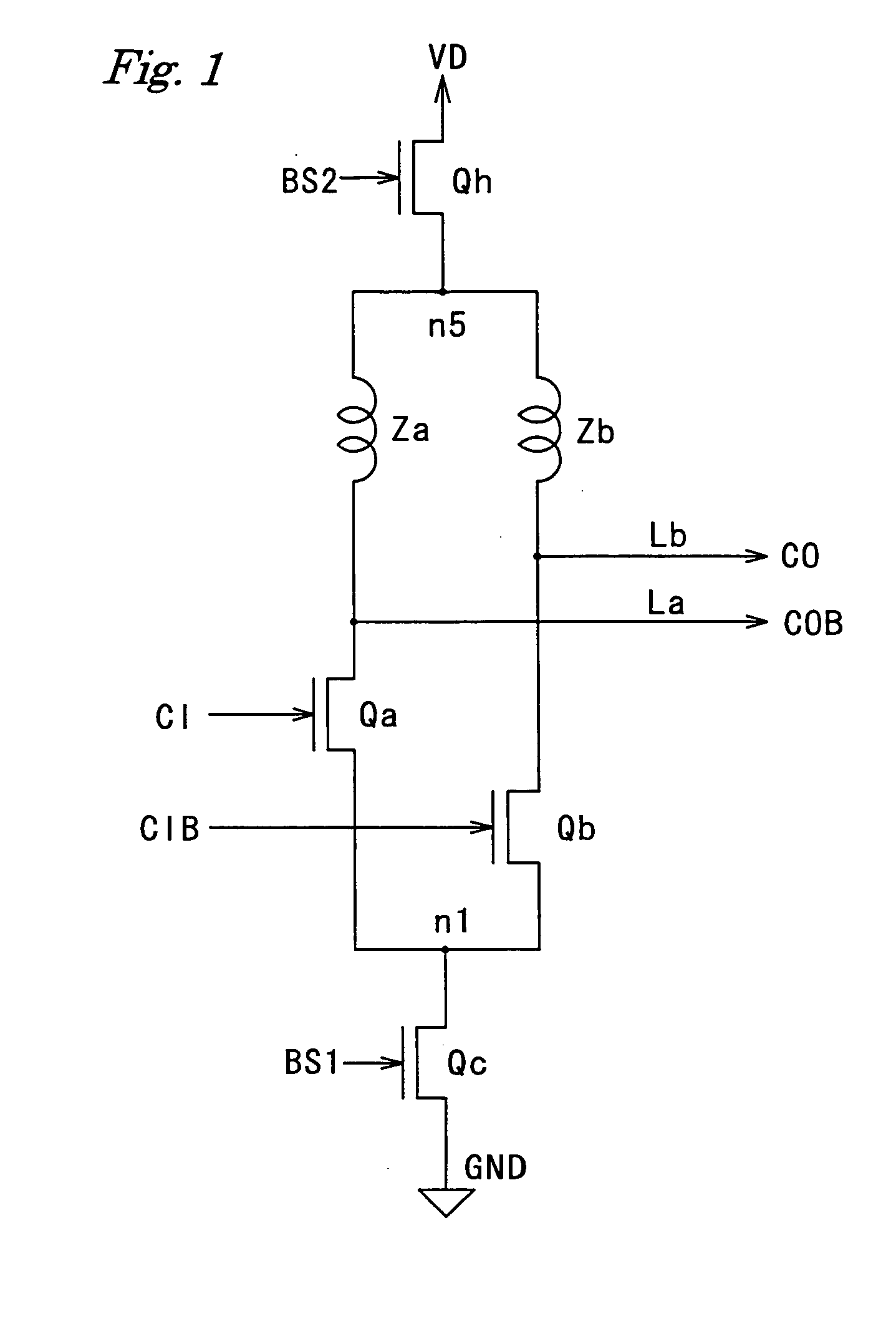
[0062]FIG. 1 is a circuit diagram showing a first embodiment according to the present invention. Here, a clock buffer circuit is exemplified for a current-mode logic (CML) circuit. Field effect transistors (FETs) Qa and Qb constitute a differential transistor pair, to which differential signals are supplied, where the gate of the FET Qa is supplied with a clock signal CI and the gate of the FET Qb is supplied with an inverted clock signal CIB.

[0063] Each source of the FETs Qa and Qb is connected in common to each other at a source node n1. Between the source node n1 and a ground line GND connected is an FET Qc for current-limiting. The gate of the FET Qc is supplied with a constant bias voltage BS1. The FETs Qa, Qb and Qc may be composed of, for example, n-MOS transistors, which can constitute a typical differential amplifier circuit.

[0064] A load circuit Za is connected to the drain of the FET Qa. Another load circuit Zb is connected to the drain of the FET Qb. Each power line si...

embodiment 2

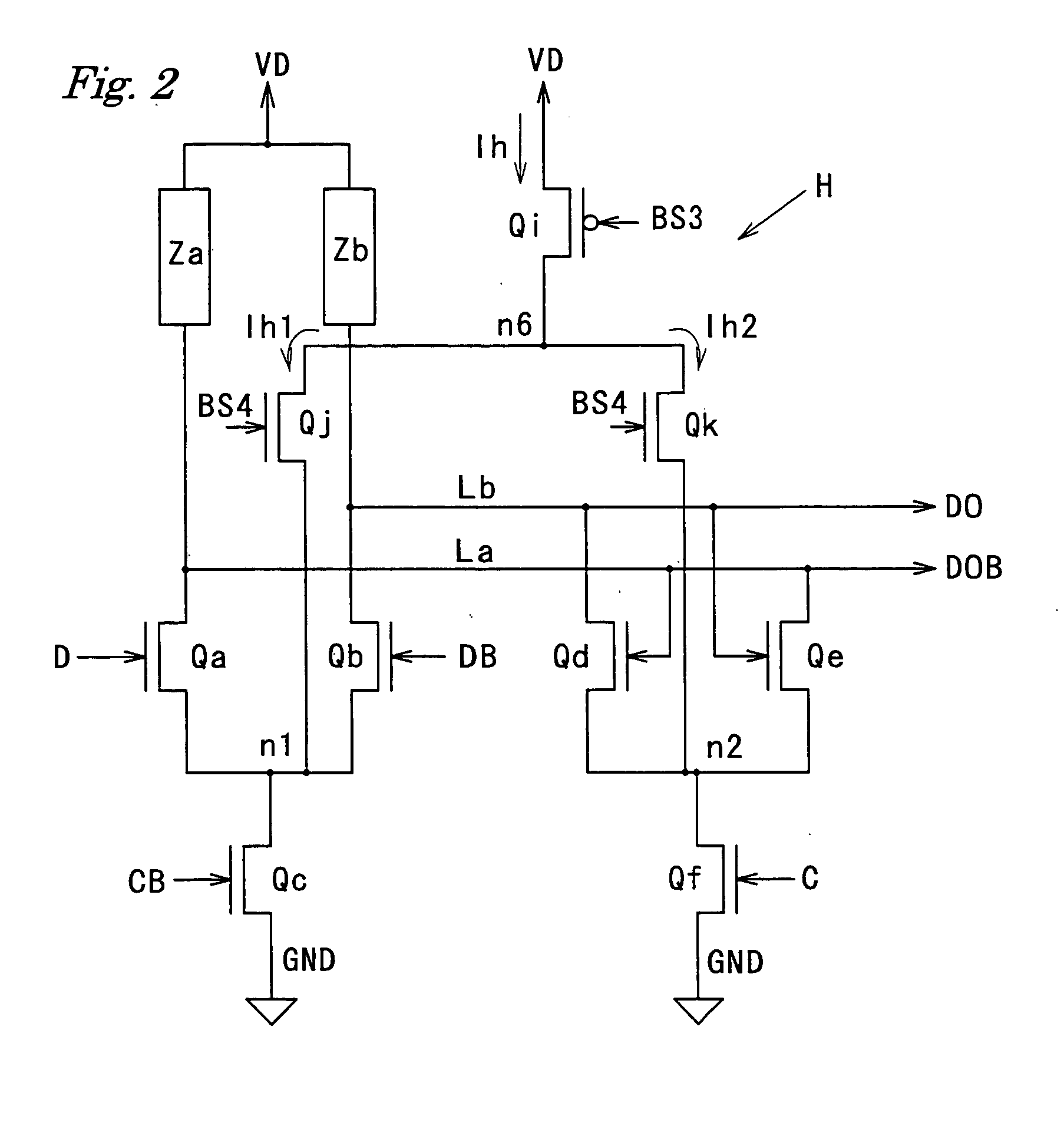
[0070]FIG. 2 is a circuit diagram showing a second embodiment according to the present invention. Here, a latch circuitry, that is a half of a D-type flip-flop circuit, is exemplified for a current-mode logic circuit. Field effect transistors (FETs) Qa and Qb constitute a differential transistor pair, to which differential signals are supplied, where the gate of the FET Qa is supplied with a data signal D and the gate of the FET Qb is supplied with an inverted data signal DB.

[0071] A load circuit Za is connected between the drain of the FET Qa and a power supply line VD. Another load circuit Zb is connected between the drain of the FET Qb and the power supply line VD. Each source of the FETs Qa and Qb is connected in common to each other at a source node n1. An FET Qc for clock-switching is connected between the source node n1 and a ground line GND. The gate of the FET Qc is supplied with an inverted clock signal CB.

[0072] An output line La is connected to the drain of the FET Qa ...

embodiment 3

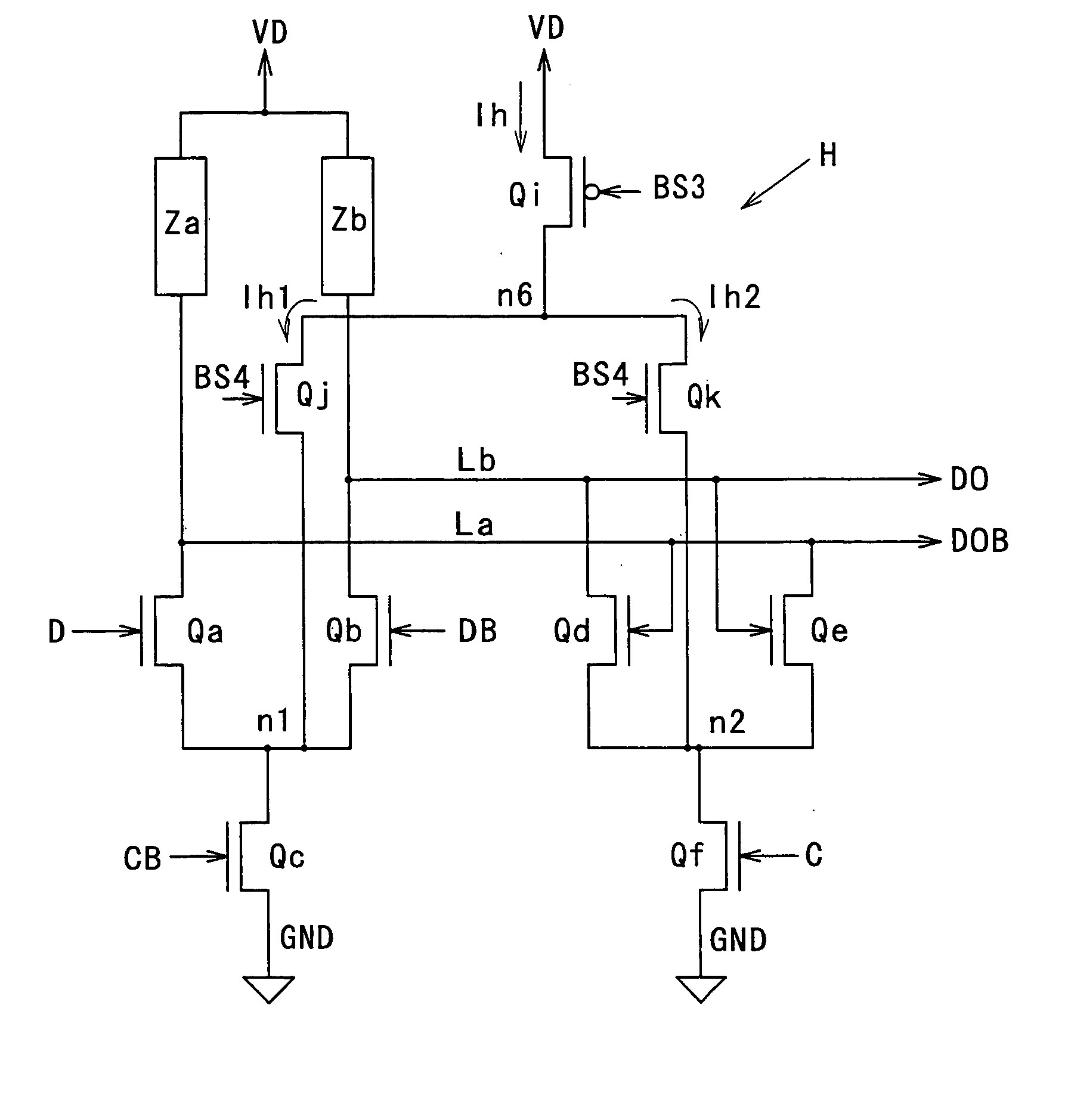
[0085]FIG. 3 is a circuit diagram showing a third embodiment according to the present invention. Here, a latch circuitry, that is a half of a D-type flip-flop circuit, is exemplified for a current-mode logic circuit. Additionally, in the current bridge circuit H as shown in FIG. 2, the FETs Qi, Qj and Qk are diode-connected so as to omit bias circuits for generating the bias voltages BS3 and BS4.

[0086] FETs Qa and Qb constitute a differential transistor pair, to which differential signals are supplied, where the gate of the FET Qa is supplied with a data signal D and the gate of the FET Qb is supplied with an inverted data signal DB.

[0087] A load circuit Za is connected between the drain of the FET Qa and a power supply line VD. Another load circuit Zb is connected between the drain of the FET Qb and the power supply line VD. Each source of the FETs Qa and Qb is connected in common to each other at a source node n1. An FET Qc for clock-switching is connected between the source nod...


PUM


Abstract

A current-mode logic (CML) circuit includes: a first field effect transistor (FET) operable based on a digital signal; a second FET operable based on an inverted digital signal; a first load circuit connected to the drain of the first FET; a second load circuit connected to the drain of the second FET; a first current limiter circuit connected between a ground line and a source node, at which the sources of the first and second FETs are connected in common; and a second current limiter circuit connected between a power supply line and a drain node, at which power line sides of the first and second load circuits are connected in common, so that the CML circuit can operate stably even with low voltage power supply.

Description

BACKGROUND OF THE INVENTION [0001] 1. Field of the Invention [0002] The present invention relates to a current-mode logic circuit including a differential amplifier circuit which can operate based on a differential signal. [0003] 2. Description of the Related Art [0004]FIG. 9 is a circuit diagram showing an example of a conventional current-mode logic (CML) circuit. Here, for easily understanding, a latch circuitry, that is a half of a D-type flip-flop circuit, is exemplified. Field effect transistors (FETs) Qa and Qb constitute a differential transistor pair, to which differential signals are supplied, where the gate of the FET Qa is supplied with a data signal D and the gate of the FET Qb is supplied with an inverted data signal DB. [0005] A load circuit Za is connected between the drain of the FET Qa and a power supply line VD. Another load circuit Zb is connected between the drain of the FET Qb and the power supply line VD. Each source of the FETs Qa and Qb is connected in commo...

Claims


Application Information

Patent Timeline
IPC IPC(8): H03K3/3562H03K17/041H03K17/693H03K19/094H03K19/0952
CPCH03K19/09432H03K17/04106
Inventor CHEN, DANIEL YU-HUA
Owner MITSUBISHI ELECTRIC CORP
Why Eureka
Try Eureka