Method of manufacturing touch sensor with switch tape strips

a technology of resistive coating and switch tape, which is applied in the direction of static indicating devices, instruments, transportation and packaging, etc., can solve the problems of resistive coating degradation, small cracks in the resistive coating, and the uniform resistivity of the coating on the cover sheet is degraded

Inactive Publication Date: 2005-05-26
TE CONNECTIVITY CORP
View PDF12 Cites 34 Cited by
  • Summary
  • Abstract
  • Description
  • Claims
  • Application Information

AI Technical Summary

Benefits of technology

[0019] The method further comprises providing a tape strip with a plurality of devices. Each of the devices has first and second terminals and is configured to allow electrical current conduction from the first terminal to the second terminal when in a first state, and prevent electrical current conduction from the second terminal to the first terminal when in a second state. Diodes and transistors are examples of devices that can perform this function. The method further comprises securing the tape strip along an edge of the resistive touch region, wherein one of the first and second terminals of the devices are in electrical contact with the resistive touch region. Preferably, the method comprises securing an electrically conductive lead to the other of the first and second terminals. In one preferred embodiment, the devices are surface mounted devices. In another preferred embodiment, the devices are thin-film devices, e.g., conductive polymer devices.
[0020] In accordance with a second aspect of the present invention, another method of manufacturing a touch sensor is provided. The method comprises providing a substrate having a resistive touch region with first and second oppositely disposed edges and third and fourth oppositely disposed edges, and providing four tape strips. Each of the tape strips comprises a plurality of devices similar to those previously described. The method further comprises securing two of the tape strips along the respective first and third edges of the resistive touch region, and the other two strips along the respective second and fourth edges of the resistive touch region. The second terminals of the devices on the first two tape strips are in electrical contact with the resistive touch region, and the first terminals of the devices on the remaining two tape strips are in electrical contact with the resistive touch region. In the preferred embodiment, at least one electrically conductive lead is coupled to the first terminals of devices not connected to the touch region, and at least another electrically conductive lead is connected to the second terminals of devices not connected to the touch region. The tape strips may be advantageously supplied in a tape reel or as a sheet, in which case the tape strips can be cut therefrom.

Problems solved by technology

However, the formation of cover sheets over spherically curved resistive touchscreens and the mechanical flexing of the cover sheet for both flat and curved resistive touchscreens tend to degrade the uniform resistivity of the coating on the cover sheet.
For example, small cracks may form in the resistive coating.
Because styluses generally have sharper radii than that of fingers, thus hastening the degradation process, the resistive coating degradation problem is an even greater concern in stylus-input devices.
This benefit, however, does not come without a price, since the resistive networks required for 5-wire designs add complexity to the resistive touchscreen design and manufacturing process.
At present, however, 3-wire and 7-wire resistive touchscreens have not gained commercial acceptance, mainly because no one has developed a low-cost means to mount the diodes or transistors onto the rigid substrate, which otherwise would involve hours of manual soldering of many discrete components onto the substrate.

Method used


Image

  • Method of manufacturing touch sensor with switch tape strips
  • Method of manufacturing touch sensor with switch tape strips
  • Method of manufacturing touch sensor with switch tape strips

Examples


Embodiment Construction

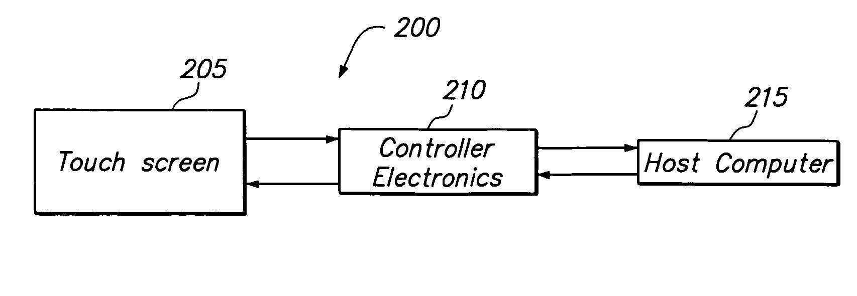
[0051] Referring to FIG. 6, a resistive touchscreen system 200 constructed in accordance with a preferred embodiment of the present invention is described. The touchscreen system 200 generally comprises a touchscreen 205 (i.e., a touch sensor having a transparent substrate), controller electronics 210, and a display (not shown). The touchscreen system 200 is typically coupled to a host computer 215. Generally, the controller electronics 210 send excitation signals to the touchscreen 205 and receive analog signals carrying touch information from the touchscreen 205. Specifically, the controller electronics 210 establish voltage gradients across the touchscreen 205. The voltages at the point of contact are representative of the position touched. The controller electronics 210 digitize these voltages and transmit these digitized signals, or touch information in digital form based on these digitized signals, to the host computer 215 for processing.

[0052] Referring now to FIG. 7, the to...


PUM

PropertyMeasurementUnit
electrical current conductionaaaaaaaaaa
electrically conductiveaaaaaaaaaa
conductiveaaaaaaaaaa

Abstract

The present invention is directed to touch sensors with arrays of switches (e.g., diodes or transistors) that can be used to selectively apply voltage gradients across a resistive touch regions of the touch sensor substrate. Touches on the touch sensor can then be sensed by measuring the voltage at the touch location on the resistive touch region. The switch arrays take the form of strips of switches that can be cut from a prefabricated reel or a sheet and applied to the touchscreen substrate.

Description

FIELD OF THE INVENTION [0001] The field of the present invention relates to touch sensor technology, and more particularly to resistive and capacitive touch sensor technology. BACKGROUND OF THE INVENTION [0002] Touch sensors are transparent or opaque input devices for computers and other electronic systems. As the name suggests, touch sensors are activated by touch, either from a user's finger, a stylus or some other device. Transparent touch sensors, and specifically touchscreens, are generally placed over display devices, such as cathode ray tube (CRT) monitors and liquid crystal displays, to create touch display systems. These systems are increasingly used in commercial applications such as restaurant order entry systems, industrial process control applications, interactive museum exhibits, public information kiosks, pagers, cellular phones, personal digital assistants, and video games. [0003] The dominant touch technologies presently in use are resistive, capacitive, infrared, a...

Claims


Application Information

Patent Timeline
Patent Type & Authority Applications(United States)
IPC IPC(8): B32B15/04G06F3/033G06F3/045
CPCY10T428/28G06F3/045
Inventor GOMES, PAULO IRULEGUIHANSEN, ERLINGTAMAKI, RYOELLSWORTH, MARK W.LLOYD, RICHARD
Owner TE CONNECTIVITY CORP
Why Eureka
Try Eureka