Thin film transistor substrate using horizontal electric field and fabricating method thereof

a thin film transistor and electric field technology, applied in the field of liquid crystal display, can solve the problems of limited cost reduction, complicated fabrication process of four-round mask, and major cost factor in the fabrication of thin film transistor substrate, and achieve the effect of improving lift-off ability and simplifying the fabrication process

Active Publication Date: 2005-05-26
LG DISPLAY CO LTD
View PDF6 Cites 25 Cited by
  • Summary
  • Abstract
  • Description
  • Claims
  • Application Information

AI Technical Summary

Benefits of technology

[0025] Accordingly, it is an object of the present invention to provide a thin film transistor substrate using a horizontal electric field and a fabricating method thereof that has a simplified fabricating process.
[0026] Another object of the present invention is to provide a thin film transistor substrate using a horizontal electric field and a fabricating method thereof that has improved lift-off ability.

Problems solved by technology

In a horizontal electric field type liquid crystal display, the complicated fabrication of the thin film transistor substrate is a major cost factor in the manufacturing of the liquid crystal display panel because it involves a plurality of masking processes.
However, since the four-round mask process still is a complicated fabricating process.
Thus, cost reduction is limited.

Method used


Image

  • Thin film transistor substrate using horizontal electric field and fabricating method thereof
  • Thin film transistor substrate using horizontal electric field and fabricating method thereof
  • Thin film transistor substrate using horizontal electric field and fabricating method thereof

Examples


Embodiment Construction

[0043] Reference will now be made in detail to the preferred embodiments of the present invention, examples of which are illustrated in the accompanying drawings.

[0044] Hereinafter, the exemplary embodiments of the present invention will be described in detail with reference to FIGS. 4 to 10D.

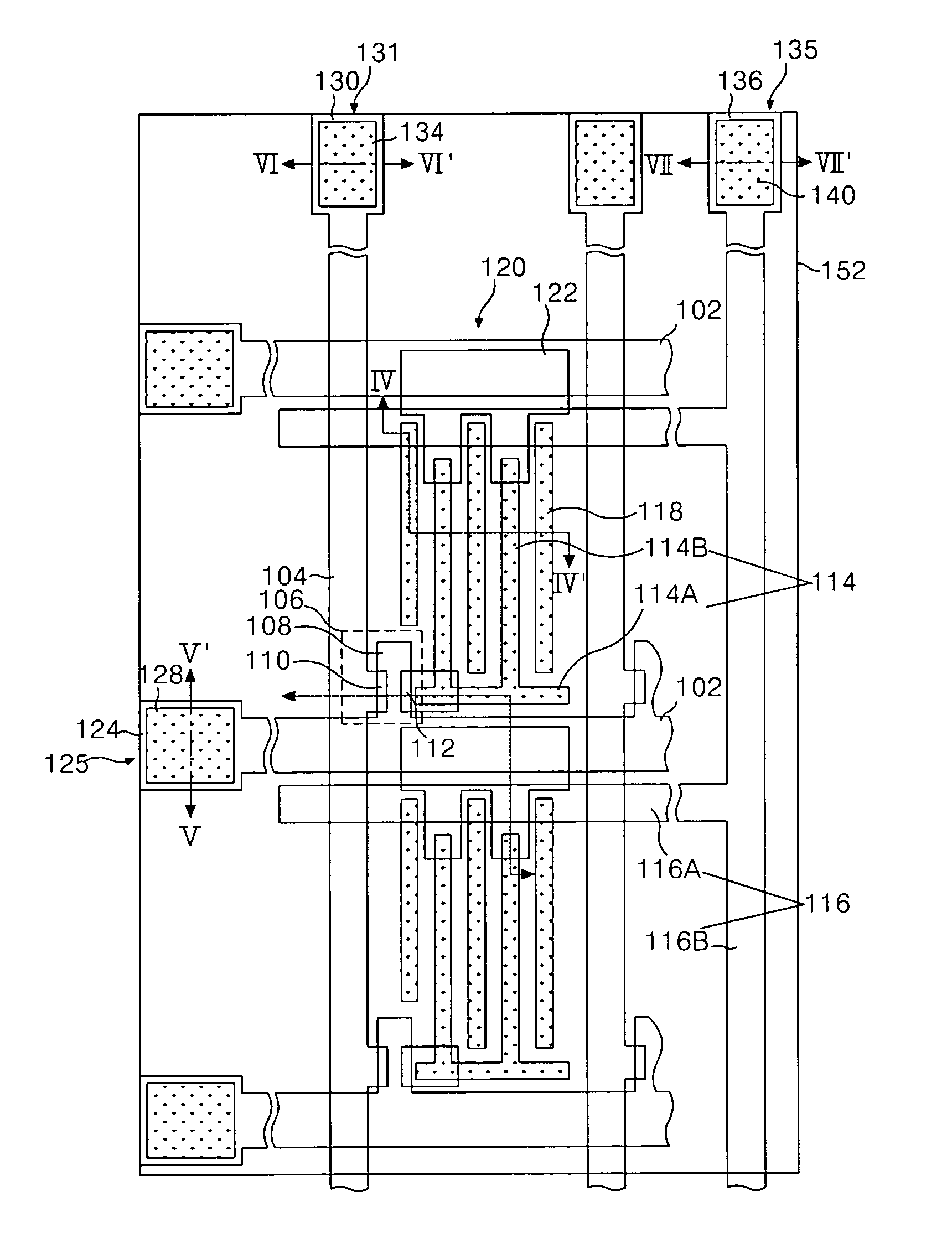
[0045]FIG. 4 is a plan view showing a structure of a thin film transistor substrate of horizontal electric field applying type according to an embodiment of the present invention. FIG. 5 is a cross-sectional view of the thin film transistor substrate taken along cross-sectional lines III-III′, IV-IV′, V-V′, VI-VI′ and VII-VII′ of FIG. 4.

[0046] Referring to FIG. 4 and FIG. 5, the thin film transistor substrate includes a gate line 102 and a data line 104 provided on a lower substrate 145 to intersect each other with a gate insulating film 146 therebetween, a thin film transistor 106 provided at each intersection, a pixel electrode 114 and a common electrode 118 in a pixel area defined by the ...


PUM

PropertyMeasurementUnit
electric fieldaaaaaaaaaa
conductiveaaaaaaaaaa
insulatingaaaaaaaaaa

Abstract

A thin film transistor substrate structure for using a horizontal electric field includes a substrate; a gate line and a common line formed parallel with each other from a first conductive layer on the substrate; a gate insulating film formed on the substrate, the gate line and the first common line; a data line formed from a second conductive layer on the gate insulating film, the data line crossing the gate line and the common line to define a pixel area; a thin film transistor connected to the gate line and the data line; a protective film covering the data line and the thin film transistor; a common electrode formed connected to the common line from a third conductive layer, the common electrode being disposed within a first hole through the protective film and the gate insulating film; and a pixel electrode connected to the thin film transistor and formed from a third conductive layer, the pixel electrode being disposed within a second hole through the protective film and the gate insulating film at the pixel area, the pixel electrode and the common electrode being disposed to define a horizontal electric field.

Description

[0001] This application claims the benefit of the Korean Patent Application No. 2003-77662 filed on Nov. 4, 2003, which is hereby incorporated by reference. BACKGROUND OF THE INVENTION [0002] 1. Field of the Invention [0003] The present invention relates to a liquid crystal display, and more particularly to a thin film transistor substrate using a horizontal electric field and a fabricating method thereof. [0004] 2. Description of the Related Art [0005] Generally, liquid crystal display (LCD) devices control light transmittance of liquid crystal using an electric field, to thereby display a picture. The liquid crystal displays are largely classified into a vertical electric field type and a horizontal electric field type depending upon the direction of the electric field driving the liquid crystal. The vertical electric field type drives a liquid crystal in a twisted nematic (TN) mode with a vertical electric field formed between a pixel electrode and a common electrode arranged in ...

Claims


Application Information

Patent Timeline
Patent Type & Authority Applications(United States)
IPC IPC(8): G02F1/1343H01L29/786G02F1/1362
CPCG02F1/134363G02F2001/136295G02F1/136286G02F1/13439G02F1/136295H01L29/786
Inventor YOO, SOON SUNGCHO, HEUNG LYUL
Owner LG DISPLAY CO LTD
Why Eureka
Try Eureka