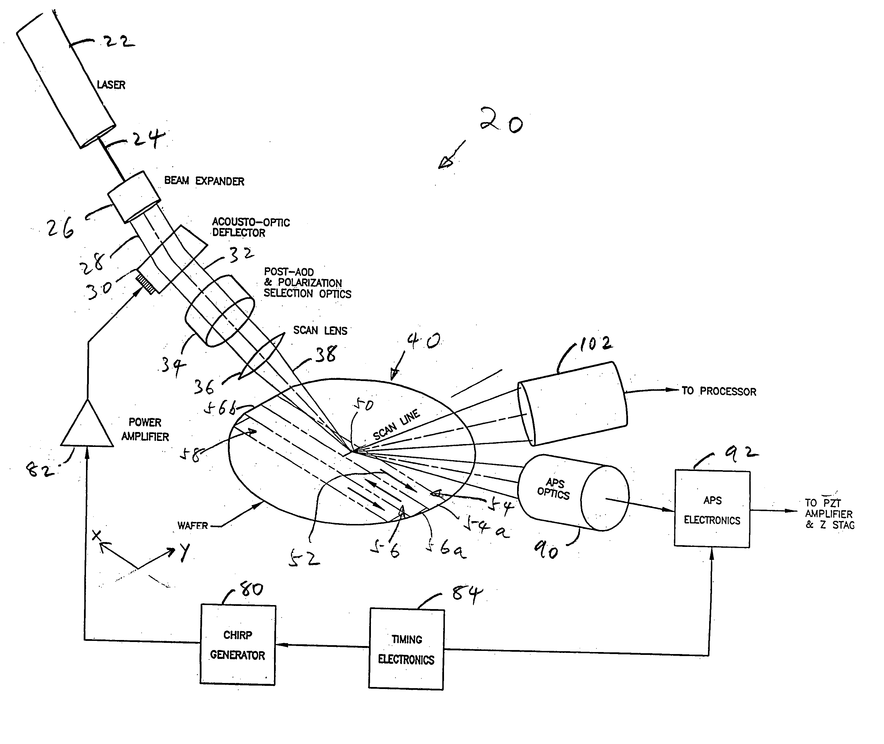
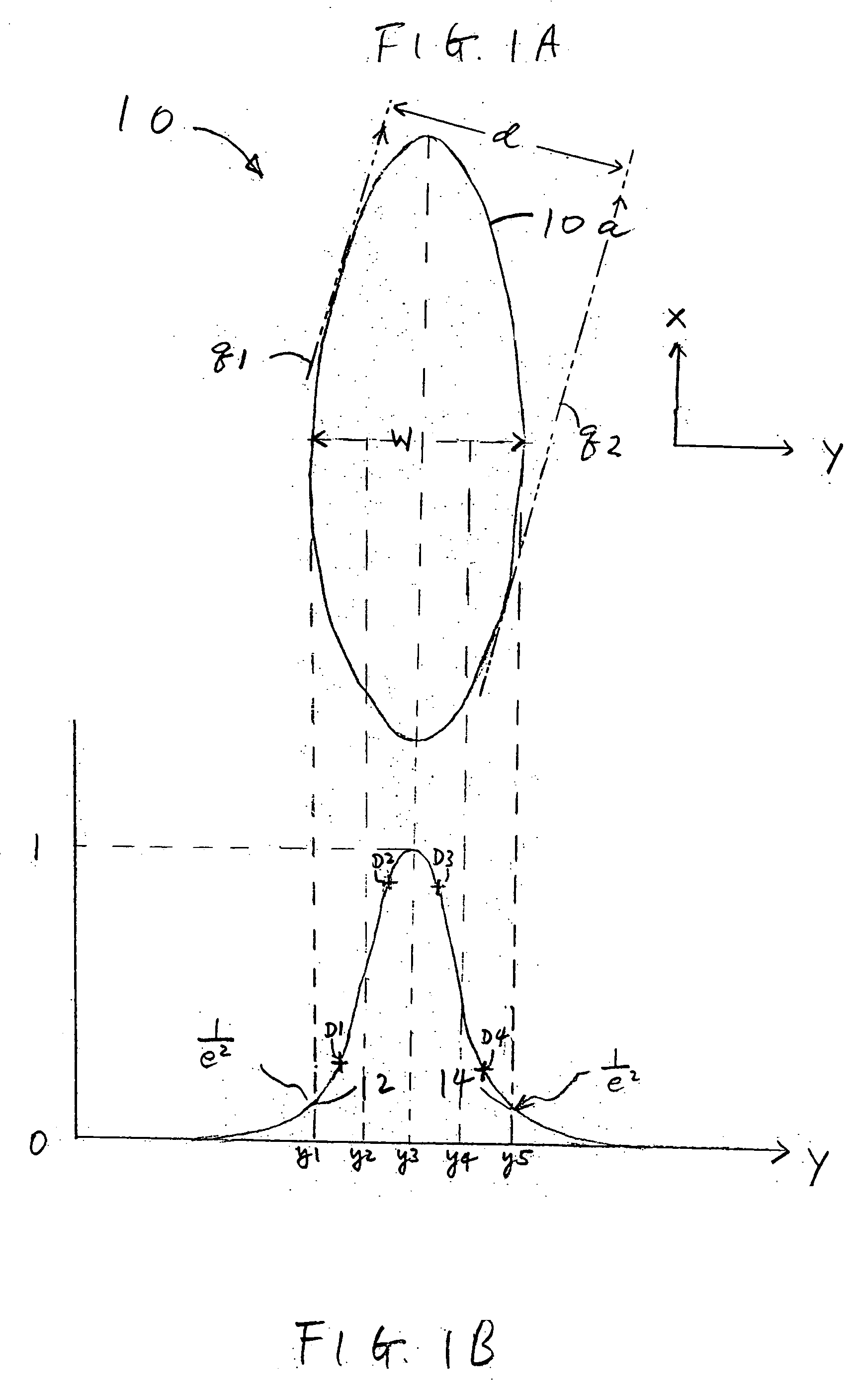
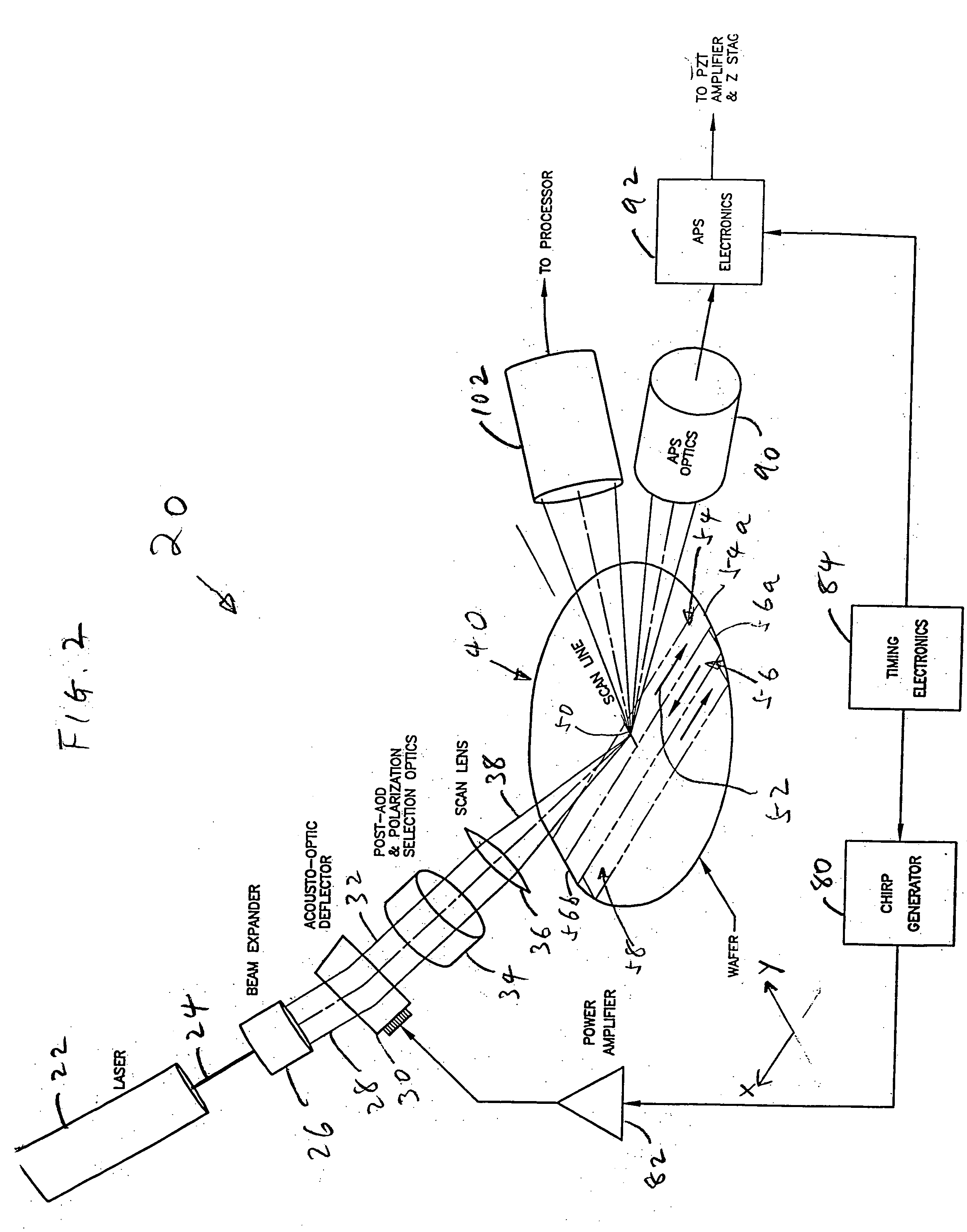
[0006] This invention is based on the recognition that very small anamolies can be detected by reducing the size of the area that is illuminated by the scanning light beam. Light scattered from structures in the spot will include background, such as light scattered by pattern on the surface, as well as light that is scattered by anomalies such as contaminant particles, pattern defects or imperfections of the surface. Such background can have a significant amplitude. For this reason, if the anamoly is of a size which is small compared to the size of the illuminated area, the scattered light from such anamoly may be overwhelmed by and become undetectable from the background. By reducing the size of the illuminated area or spot size, the ratio of the light intensity scattered by an anomaly to that of the background will be increased, thereby increasing detection sensitivity. However, with a smaller spot size, it will be more difficult to maintain the uniformity of the spot along a long straight scan line across the entire wafer. By breaking up the scan path into short segments, it is possible to employ a smaller spot size while at the same time maintaining uniformity of the spot along the path. From the system point of view, by reducing the length of the scan, the size of the collection optics for detecting forward scattered light becomes more manageable.
[0009] Another consideration of the invention is to provide an adequate throughput while data is collected at a moderate rate for defect detection so that the data collection and processing system employed need not be overly complex and expensive.
[0017] It is a further object of the present invention to classify detected anomalies and determine their size while increasing the confidence and accuracy of the detection system by reducing false counts.
[0018] These objects have been achieved with an apparatus and method for detecting anomalies of sub-micron size, including pattern defects and particulate contaminants, on both patterned and unpatterned wafer surfaces. For the purposes of this application, a particulate contaminant is defined as foreign material resting on a surface, generally protruding out of the plane of the surface. A pattern defect is in the plane of the surface and is usually induced by contaminants during a photolithographic processing step. The device employs a plurality of collector channels symmetrically disposed, in the azimuth, on opposite sides of the center of a scan line. In addition to the collector channels, other detector channels are employed to enhance the detection of anomalies. The collector and detector channels are collectively referred to as inspection channels. Also, an interchannel communication apparatus is employed to compare and adjust data received from each of the inspection channels which facilitate detecting and characterizing anomalies. A laser beam illuminates a localized spot on a wafer surface with the beam having a grazing angle of incidence, and the spot is scanned over a short scan line. The wafer is orientated so that the streets of the patterns on the die are not oblique with respect to the scan line, i.e., the streets are either perpendicular or parallel to the scan line. The surface is moved in a serpentine fashion, along adjacent striped regions, as the spot is scanned over its entire area. The position of the inspection channels, as well as the polarization of the beam, allows distinguishing, inter alia, pattern defects from particulate contaminants. The detector channels include an imaging channel which combines the advantages of a scanning system and an imaging system while improving signal / background ratio of the present system. The inspection channels collect light and feed it to a light detector for producing an electrical signal corresponding to the collected light intensity. The interchannel communication apparatus is a processor which stores, in memory, the information carried by the signals from the inspection channels, with the memory addresses corresponding to spatial positions on the surface. The processor constructs maps from the stored information, representing the anomalies detected on the surface. The maps from the inspection channels are compared by performing various algorithms and logical operations, e.g., OR, AND and XOR, to characterize the detected anomalies.
[0019] In operation, each wafer is scanned with a beam incident thereon at a grazing angle and the light scattered and specularly reflected from the wafer's surface are simultaneously collected with the above mentioned inspection channels. Previously, the wafer has been aligned so that the streets on the die are not oblique with respect to the scan line. Light collected is converted into electrical signals which are further processed by dedicated electronics. A processor analyzes the information carried by the signals and produces various maps representing the light intensity detected at various beam positions. The maps are compared either in the analog domain or digitally to identify and characterize anomalies. If compared digitally, the maps are binarized which allows performing various algorithmic and logical, e.g. OR, AND and XOR, operations on the data they represent, thereby allowing a user to choose a desired level of confidence in the detected anomalies. The binarization can take place against either a constant or a variable threshold, further reducing the occurrence of false counts. The variable threshold is dependent upon the local reflectivity and can be derived from a reflectivity channel which determines local reflectivity of the surface based upon detecting specularly reflected light.
[0020] The invention has advantages over the previous scanning techniques in that it provides a small spot that scans at speeds far in excess of those of the prior art, while providing the added feature of classifying anomalies. Further, controlling the polarization of the incident beam and the light detected results in an excellent ratio of particle to pattern signal.