Optical broad band element and process for its production

a broad band element and optical technology, applied in the direction of instruments, lighting and heating apparatus, nuclear engineering, etc., can solve the problems of changing parameters, less suited, and system saturated with hydrogen

Inactive Publication Date: 2005-05-26
CARL ZEISS SMT GMBH
View PDF6 Cites 15 Cited by
  • Summary
  • Abstract
  • Description
  • Claims
  • Application Information

AI Technical Summary

Benefits of technology

[0033] In case the layer formed of material C is an artificial layer that has an effect as an barrier layer so that no interdiffusion effects between the multilayer material can occur, it is preferred to use Mo5Si3, Si3N4, Rh5Si3, Rh2Si, RhSi, Ru2Si, Ru2Si, RuS1, MO2C, SiC, Nb4Si, Nb5Si3, Y5Si3, YSi, YSi2, diamond-like C, Zr2Si, Zr5Si3, MoB, B4C or B.

Problems solved by technology

On conversion to actual optical broad band elements however there occur a number of problems.
For mass-production of optical broad band elements e.g. for use in lithography, this approach is less suited, as constant working with hydrogen is connected with an increased risk of explosion.
Also system saturated with hydrogen are not very stable and changing their parameters with time.
Another problem arises in that oxide strata or adhesive layers can form on the surface of the broad band element, which also have a negative effect on the reflectivity performance.
As a result the angular or wavelength reflectivity profile of the broad band element becomes strongly distorted leading to unacceptable deviation from the desired reflectivity response.
These deviations of the actual multilayer systems from the calculated multilayer systems lead to reflectivity losses of several percent.
This is particularly detrimental to the use of optical broad band elements in lithography, as a large number of optical elements are successively linked in series in lithography systems.

Method used


Image

  • Optical broad band element and process for its production
  • Optical broad band element and process for its production
  • Optical broad band element and process for its production

Examples


example 1

[0049] For producing a broad band reflector for a wavelength of 13.4 nm and an angle band width of 20°, molybdenum carbide and silicon were chosen as materials. Molybdenum carbide and silicon are two materials which do not interact. Silicon was also chosen as cap layer material. No adhesive stratum forms on silicon, but simply a negligibly thin silicon dioxide stratum, should the broad band reflector not be kept in a vacuum. Both silicon and molybdenum carbide, on the basis of their absorption coefficient, are suitable for the production of optical elements in the extreme ultra violet wavelength range.

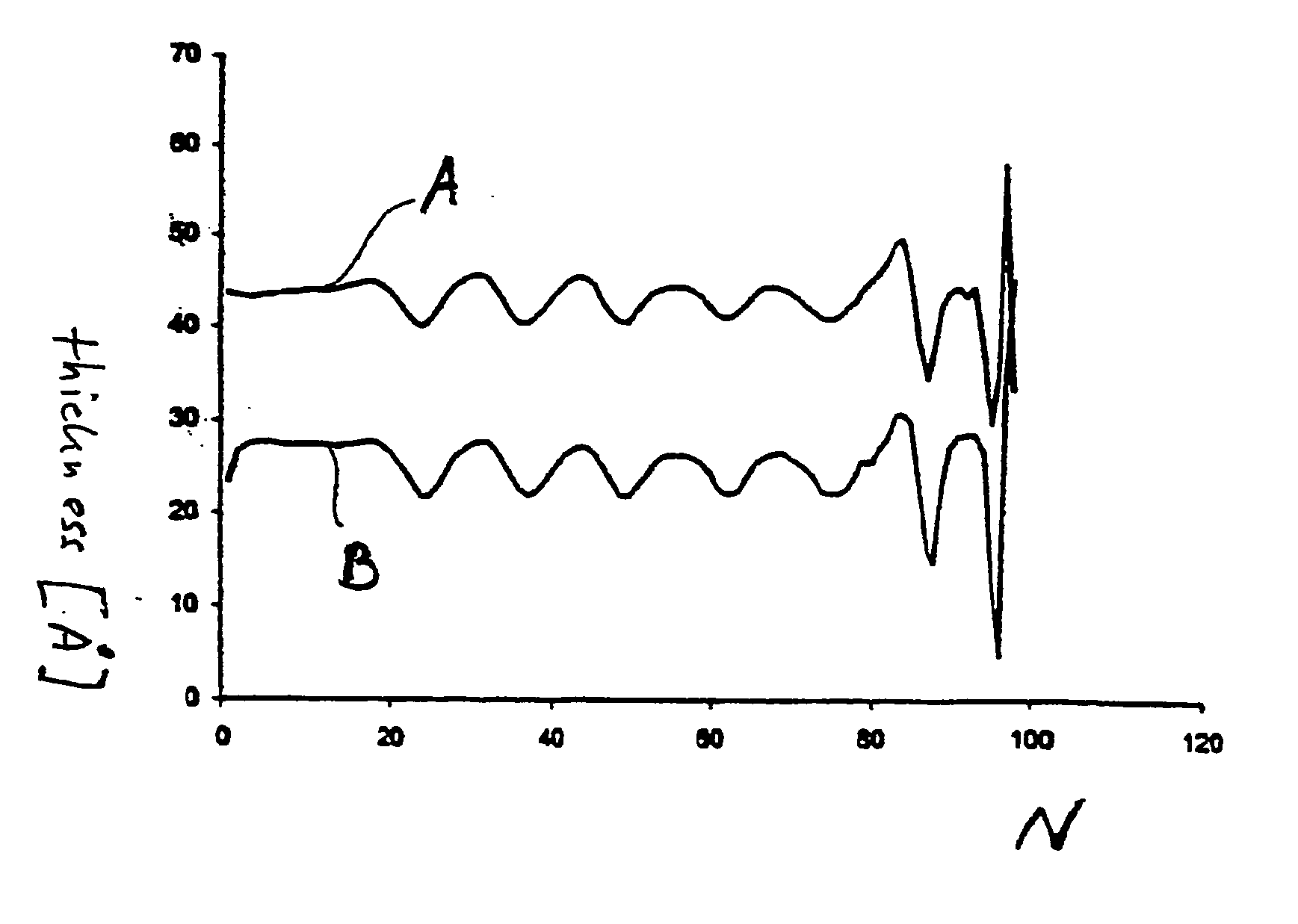
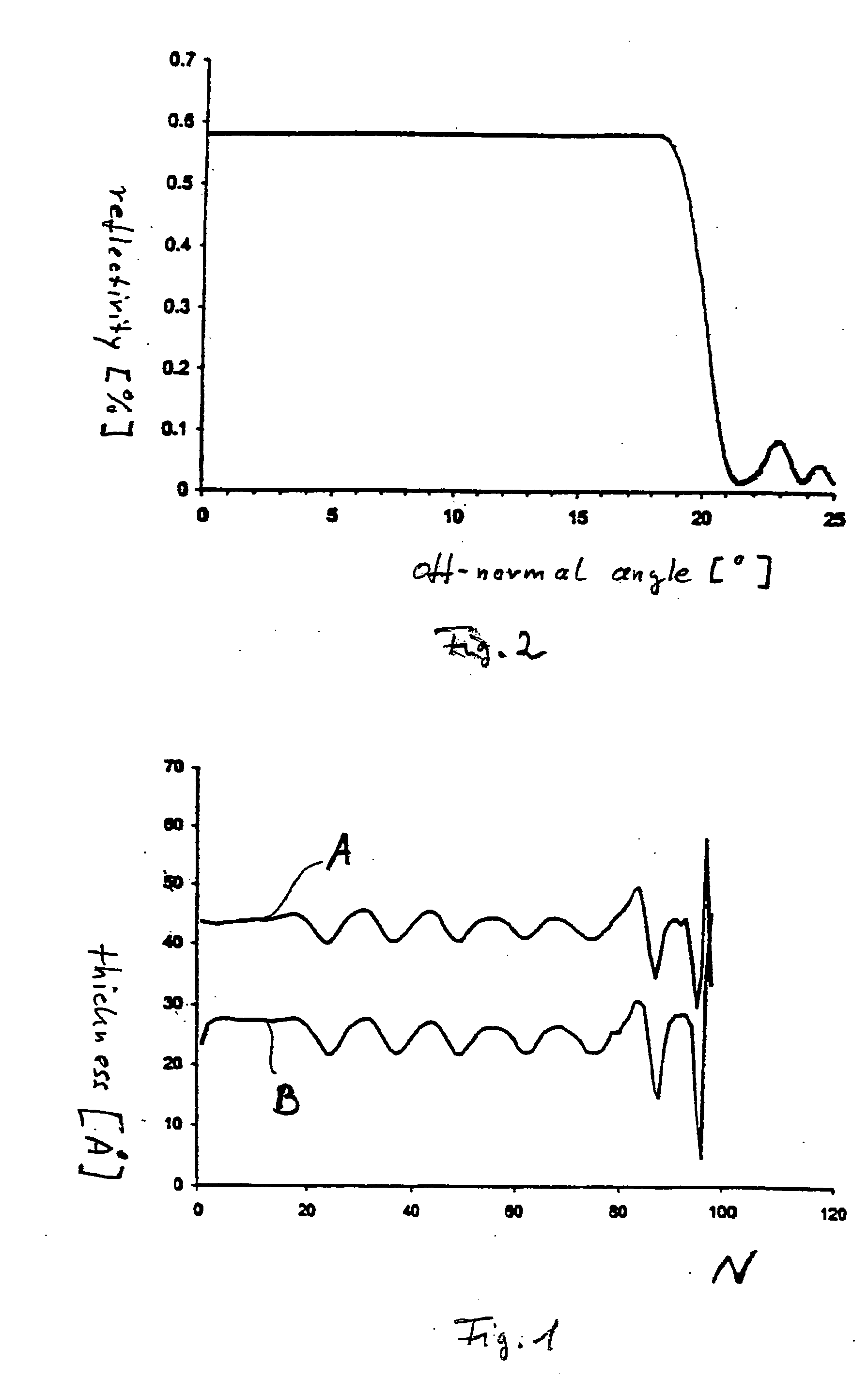
[0050] Given a set or period number N=100 and a layer thickness distribution which was obtained according to E. Ziegler et al., the thickness distribution was optimized as per P. van Loevezijn et al. Their resulting thickness distribution is represented in FIG. 1. Here the thickness is represented depending on the set number N, where counting is started at the side turned to the vacuu...

example 2

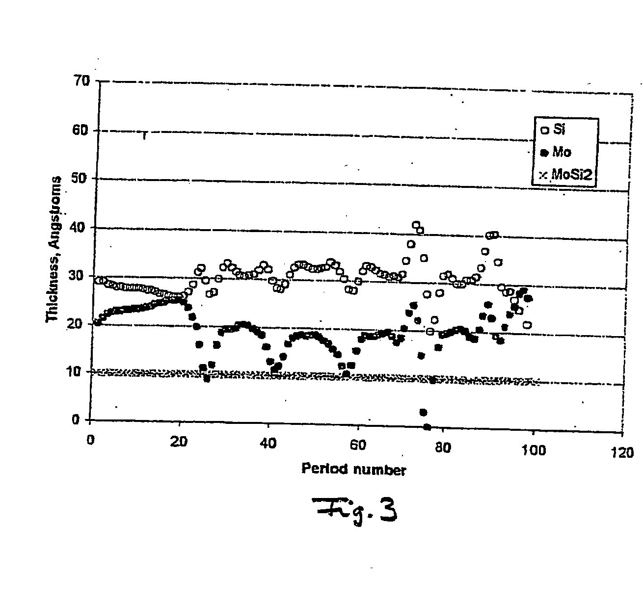
[0052] Three-material depth-graded multilayer deposited in the sequence: Mo / MoSi2 / Si / MoSi2. Design contains variable thicknesses of Mo and Si, with the thickness of MoSi2 being kept constant at 1.0 nm (FIG. 3). The structure is covered with 2.0 nm SiO2 cap layer. The structure is optimized for an even reflectivity response in the range of off-normal angles of incidence 0-18 degrees at 13.4 nm (FIG. 4). Molybdenum disilicide (MoSi2) is the most stable compound found in Mo-Si system. Therefore the deliberately introduced MoSi2 layers in the design serve as a strong diffusion barrier between Mo and Si. Top SiO2 layer provides reliable protection against oxidation of deeper layers in the structure while kept in air or vacuum. Precision of thicknesses of layers in the structure is determined by precision of a deposition method and will not be altered by interactions of materials in the structure with each other or with atmosphere.

[0053] A comparison of the reflectivity curve in FIG. 4 (...


PUM


Abstract

A process for the production of optical broad band elements for the ultra violet to hard x-ray wavelength range, especially the extreme ultra violet wavelength range is described. A set from series of layers made of at least two materials in relation to the layer sequence is designed and numerical optimization of the the layer thicknesses and of the cap layer thickness is performed. The materials are chosen in such a way that two successive layers interact with each other as little as possible or controllably. The set can be formed from MO2C— and Si-layers. The numerical optimization takes into account interlayers of a certain thickness and composition.

Description

CROSS REFERENCE [0001] This application is a continuation-in-part application of International Application No. PCT / EP03 / 03200, filed Mar. 27, 2003 and published as WO 03 / 081187 on Oct. 2, 2003, which claims the priority to European Application No. 02006984.5, filed Mar. 27, 2002.FIELD OF THE INVENTION [0002] The invention concerns a process for the production of broad band elements, especially broad band mirrors, for the ultra violet to hard x-ray wavelength range, especially the extreme ultra violet wavelength range according to the claims. The invention is also related to optical broad band elements, especially broad band mirrors. BACKGROUND OF THE INVENTION [0003] In the ultra violet to hard x-ray wavelength range, especially in the extreme ultra violet range (approx. 10 to 100 nm) multilayer systems are used for optical elements as a rule. To this end layers are arranged successively with their respectively constant thickness out of a low and high absorbent material. Here the th...

Claims


Application Information

Patent Timeline
Patent Type & Authority Applications(United States)
IPC IPC(8): G02B26/08G21K1/06
CPCB82Y10/00G21K1/062G02B26/0841
Inventor YAKSHIN, ANDREY E.KOJEVNIKOV, IGOR V.BIJKERK, FREDERIKLOUIS, ERIC
Owner CARL ZEISS SMT GMBH
Why Eureka
Try Eureka