
X-Ray Monitoring Optical Elements

a technology of optical elements and x-rays, applied in radiation/particle handling, nuclear engineering, electric devices, etc., can solve problems such as uncompensated electric charges, and achieve the effect of enhancing surface conductivity and increasing surface conductivity

Active Publication Date: 2015-04-02
UCHICAGO ARGONNE LLC
View PDF12 Cites 10 Cited by
  • Summary
  • Abstract
  • Description
  • Claims
  • Application Information

AI Technical Summary

Benefits of technology

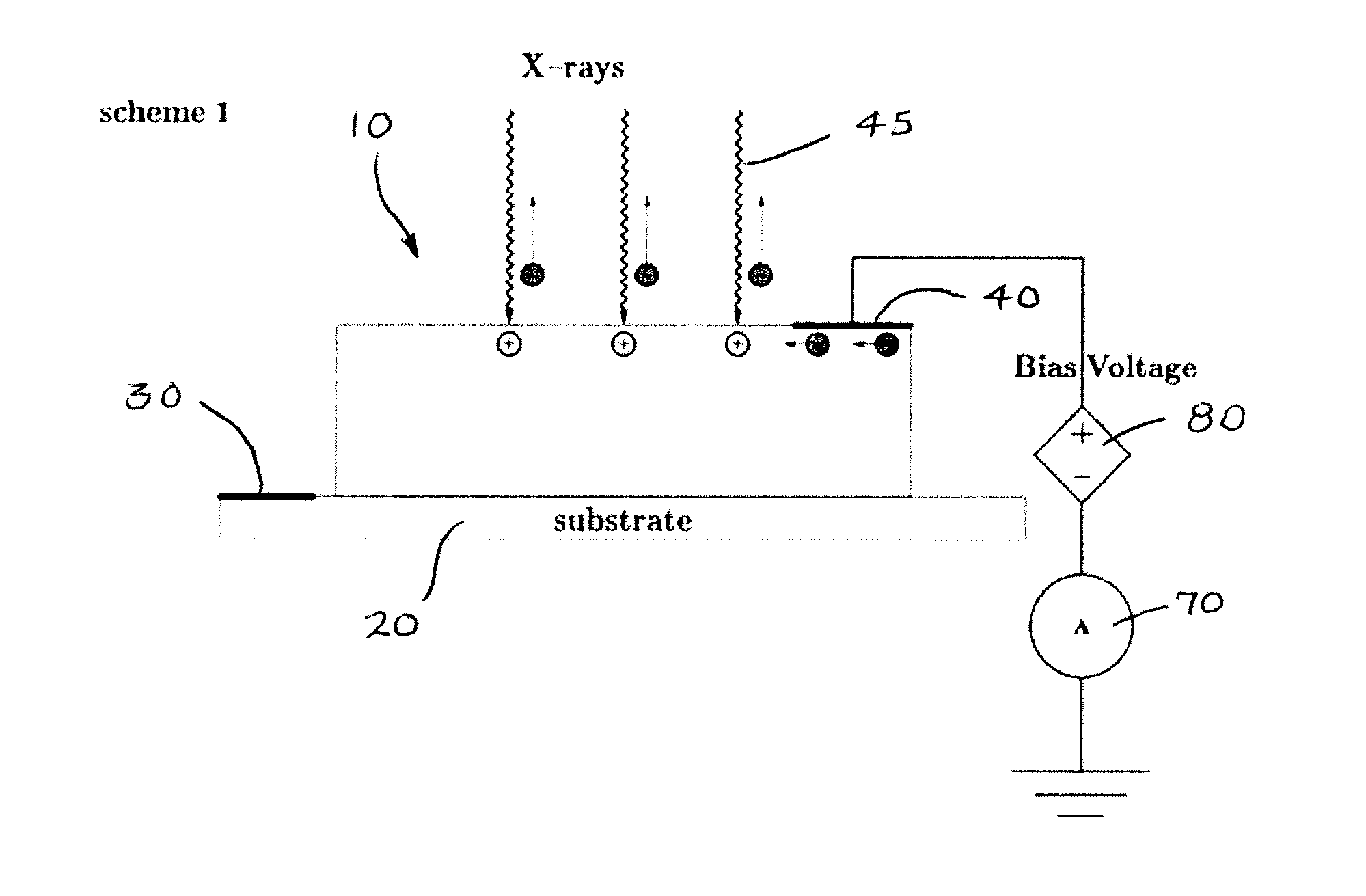
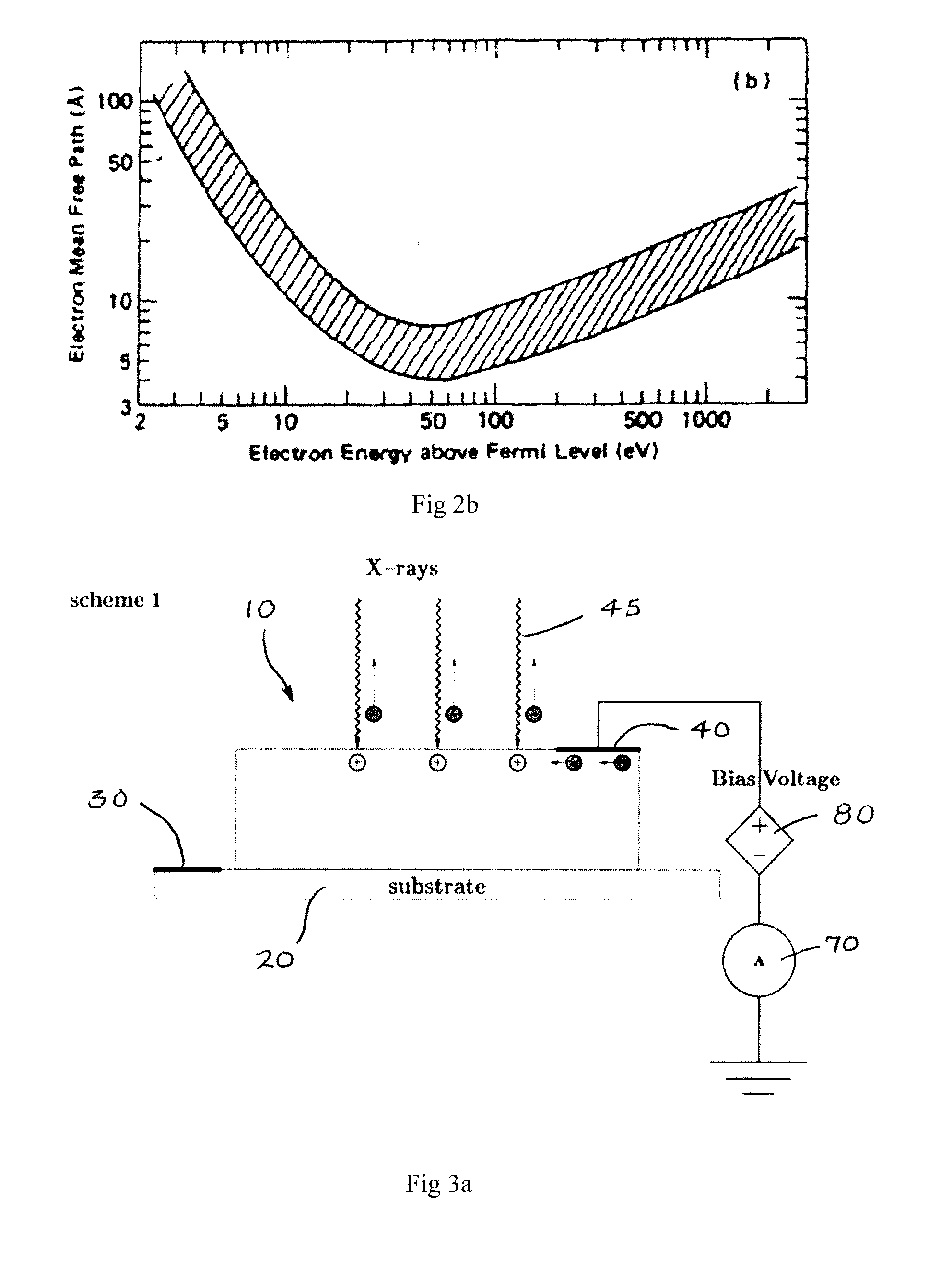
The present patent describes a method for creating a hard X-ray monitor by using X-ray induced photoemission and enhancement in surface conductivity. The energy of a hard X-ray photon is sufficient to create multiple photoionization events, resulting in an uncompensated electric charge. However, charge carriers generated by X-rays that don't escape the material can enhance its surface conductivity. As an electrical contact between the material surface and an electron supply compensates the generated surface charge, the magnitude of the electric current can serve as a measure of the incident photon flux. This method has advantages over bulk charge collection in a semiconductor device and can provide accurate and reliable detection of X-rays.

Problems solved by technology

As a result an uncompensated electric charge is generated.

Method used


Image

  • X-Ray Monitoring Optical Elements
  • X-Ray Monitoring Optical Elements
  • X-Ray Monitoring Optical Elements

Examples


example i

[0022]A quantitative description of total electron yield is provided which follows a known basic phenomenological model [see, for example, J. Stohr, NEXAFS spectroscopy, vol. 25 of Springer Series in Surface Sciences (Springer, Berlin Heidelberg New York, 1992)]. The goal is to estimate electric current due to total electron yield in several primary X-ray optical materials for hard X-rays. This consideration will lead to several important practical estimates given in Example III.

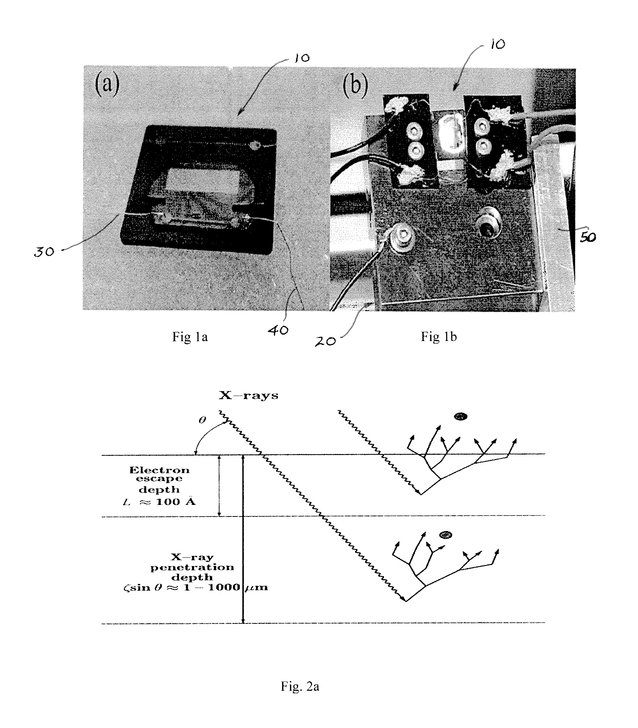
[0023]At normal incidence X-ray photons penetrate into the bulk of the material to a characteristic depth ζ (X-ray absorption length) given by the inverse of the linear attenuation coefficient μ(EX) [cm−1], which is a function of photon energy EX. The X-ray flux density f [photons / (s cm2)] transmitted through a material depth z is attenuated (with respect to an incident flux f0 according to the Beer's law

f=f0exp(−μ(EX)z).  (1)

[0024]The X-ray attenuation coefficient is related to the total X-ray attenuation c...

example ii

Quantum Yield

[0037]In this Example II particular practical cases are considered to obtain formulas for a quantum yield, which is a number of photoelectrons emitted per single incident X-ray photon of energy EX:

Q=Yf0S0=12(1-R(θ))GeLζθ+L.(7)

[0038]In grazing incidence under the condition of total external reflection (i.e., X-ray mirror case) a substantial increase in the quantum yield can be obtained. This condition is satisfied if θC where θC is the critical angle that depends on the choice of the material and incident photon energy (e.g.,). The estimate of total electron yield can be performed by replacing in Eq. (7) the X-ray penetration depth ζθ with X-ray attenuation length Λ in total external reflection. The values for Λ can be obtained using an online calculator.

[0039]The penetration depth at angle of incidence below the critical angle can be several times smaller than the effective electron escape length. Therefore an assumption Λ<<L can be applied. Under this approximation the...

example iii

[0043]Table I herebelow presents a summary of quantum yield for various X-ray optical materials. For Au the effective photoelectron escape depth was assumed L=50 Å. For other materials in the list (a dielectric C and a semiconductor Si) L=100 Å was assumed. In case of Au the value for Ge was available in the literature; and the quantum yield at a representative energy 10 keV was estimated directly from Eq. (7). For C and Si the values for electron yield relative to that of Au were given in the literature for particular energies. In these cases Ge was calculated at those energies and extrapolated to a representative energy of 10 keV.

[0044]In the case of total external reflection (TER) for Au the quantum yield can be as high as 0.6 (Au) which is due to the fact that the X-ray photon penetration depth is only about 10 Å (much less than L=50 Å). The X-ray photon penetration depth was estimated at an angle of θ=2.5 mrad, which is below the critical angle for total external reflection for...


PUM


Abstract

An X-ray article and method for analyzing hard X-rays which have interacted with a test system. The X-ray article is operative to diffract or otherwise process X-rays from an input X-ray beam which have interacted with the test system and at the same time provide an electrical circuit adapted to collect photoelectrons emitted from an X-ray optical element of the X-ray article to analyze features of the test system.

Description

STATEMENT OF GOVERNMENT INTEREST[0001]The U.S. Government has rights in this invention pursuant to Contract No. W-31-109-ENG-38 between the U.S. Government and the University of Chicago and / or pursuant to DE-AC-02-06 CH11357 between the U.S. Government and the UChicago Argonne, LLC representing Argonne National Laboratory.FIELD OF THE INVENTION[0002]This invention relates to development of a method, system and article of manufacture for X-ray monitoring by selected optical elements. More particularly the invention relates to a method, system and article of manufacture which can sense hard X-rays to generate an electrical current characteristic of the intensity of the X-ray beam and at the same time act as a diffracting element for X-ray optical systems. This methodology and system can also function in a similar manner for many classes of X-ray optics, including but not limited to reflective or mirror systems, refracting lenses and for transmission optics, such as filters, windows, a...

Claims


Application Information

Patent Timeline
IPC IPC(8): H05G1/26
CPCH05G1/265G01T1/26
Inventor STOUPIN, STANISLAVSHVYDKO, YURYKATSOUDAS, JOHNBLANK, VLADIMIR D.TERENTYEV, SERGEY A.
Owner UCHICAGO ARGONNE LLC
Learn More