Method for manufacturing conductive pattern forming body

a technology of forming body and conductive pattern, which is applied in the direction of liquid/solution decomposition chemical coating, instruments, photomechanical apparatus, etc., can solve the problems of high cost, inability to apply to manufacturing a highly precise conductive pattern, and large amount of waste liquid occurring from developing, etc., to achieve excellent conductive pattern forming body

Inactive Publication Date: 2005-05-26
DAI NIPPON PRINTING CO LTD
View PDF4 Cites 30 Cited by
  • Summary
  • Abstract
  • Description
  • Claims
  • Application Information

AI Technical Summary

Benefits of technology

[0078] Also, the present invention provides a conductive pattern forming body comprising: a base material; a wettability variable layer formed in a pattern on the base material whose wettability is changed by an action of a photocatalyst; and a metal composition formed on the wettability variable layer, by solidifying a metal colloid. By proiding the wettability variable layer on the base material, a conductive pattern forming body can be easily produced. Further, when the base material has insulating property, it is possible to form an excellent conductive pattern forming body.

Problems solved by technology

However, in such a method using photolithography method, it is necessary to pass through various processes such as plating of a substrate with a metal, formation of a photoresist layer, exposure and developing, making the method for manufacturing complicated and a cost may be a problem.
Also, a large amount of waste liquid occurring from developing is harmful, and there is an environmental problem that treatments are necessary to drain these waste liquids outside.
However, this method has a problem on precision so that it cannot be applied to the case of manufacturing a highly precise conductive pattern.

Method used


Image

  • Method for manufacturing conductive pattern forming body
  • Method for manufacturing conductive pattern forming body
  • Method for manufacturing conductive pattern forming body

Examples


first embodiment

1. First Embodiment

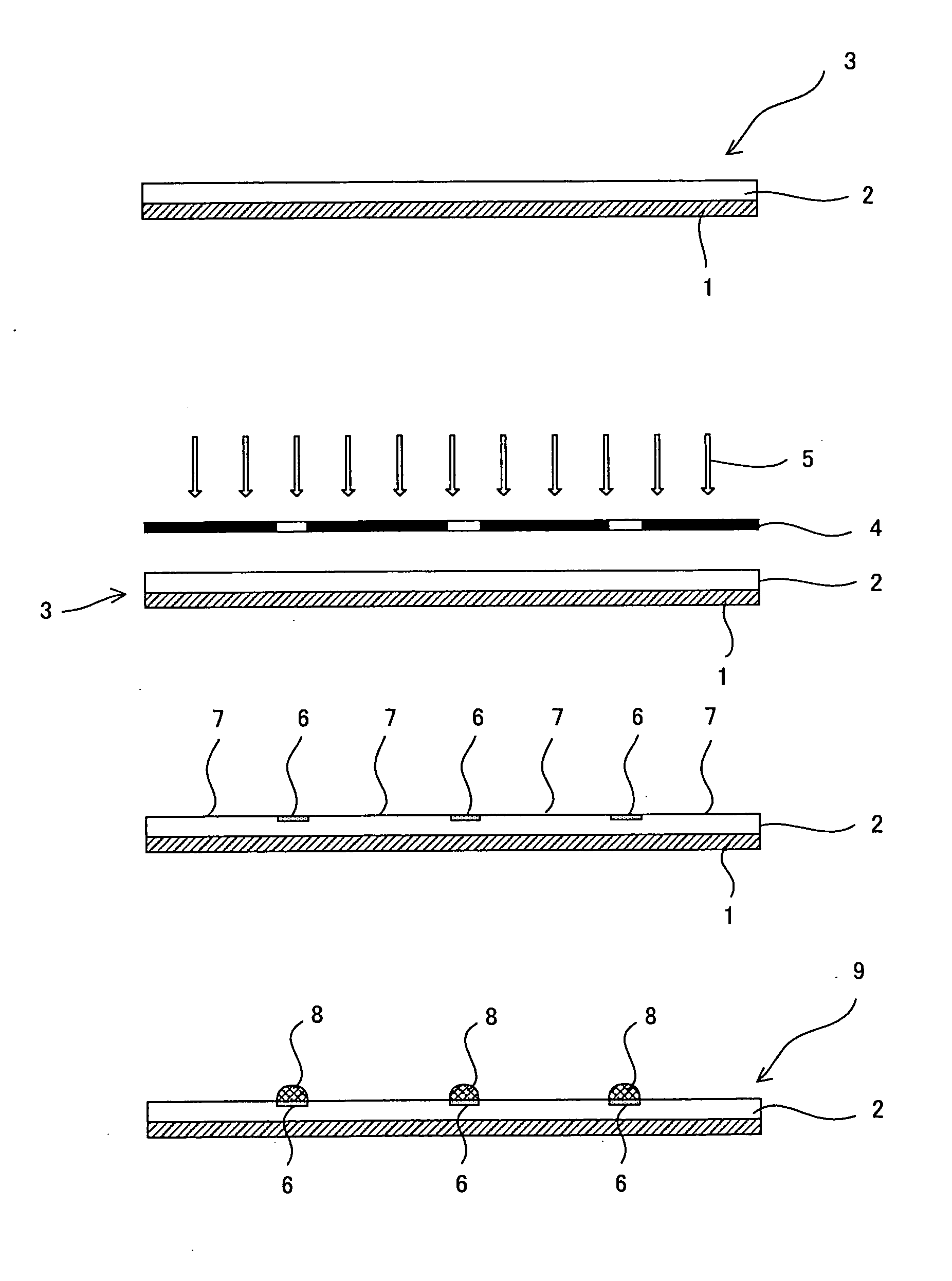
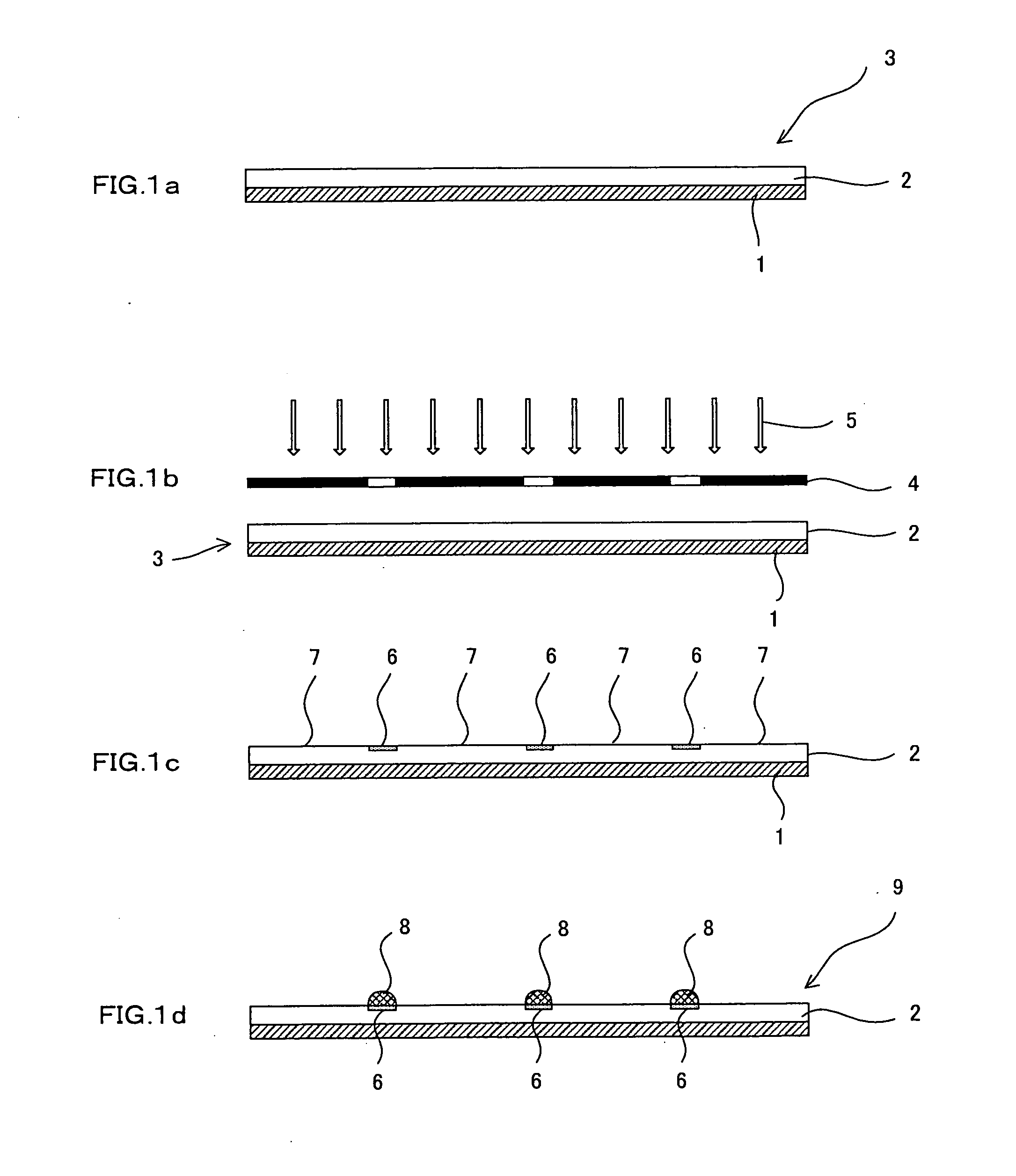
[0391] First, the first embodiment of the pattern forming body of the present invention will be explained. The first embodiment of the pattern forming body of the present invention comprises: a base material; a photocatalyst containing layer which is a layer formed on the base material whose wettability of an energy irradiated part is changed so as a contact angle to a liquid is reduced, and contains at least a photocatalyst and a binder; and a metal composition formed on the photocatalyst containing layer by solidifying a metal colloid in a pattern.

[0392] The conductive pattern forming body in this embodiment is provided with the photocatalyst containing layer, and it is therefore, possible to form a conductive pattern with ease in a small number of processes by utilizing a difference in wettability, and a conductive pattern forming body can be formed at a low cost.

[0393] Also, in a case of this embodiment, the electric resistance of the photocatalyst containin...

second embodiment

2. Second Embodiment

[0396] Next, the second embodiment of the conductive pattern forming body of the present invention will be explained. The second embodiment of the conductive pattern forming body of the present invention comprises: a base material; a photocatalyst containing layer which is a layer formed on the base material in a pattern whose wettability of an energy irradiated part is changed so as a contact angle to a liquid is reduced, and contains at least a photocatalyst and a binder; and a metal composition formed on the photocatalyst containing layer by solidifying a metal colloid.

[0397] The conductive pattern forming body of this embodiment is provided with the photocatalyst containing layer, and it is therefore, possible to form a conductive pattern with ease by utilizing a difference in wettability, and also a conductive pattern forming body can be formed at a low cost. Also, in this embodiment, since the photocatalyst containing layer is formed in a pattern, the base...

third embodiment

3. Third Embodiment

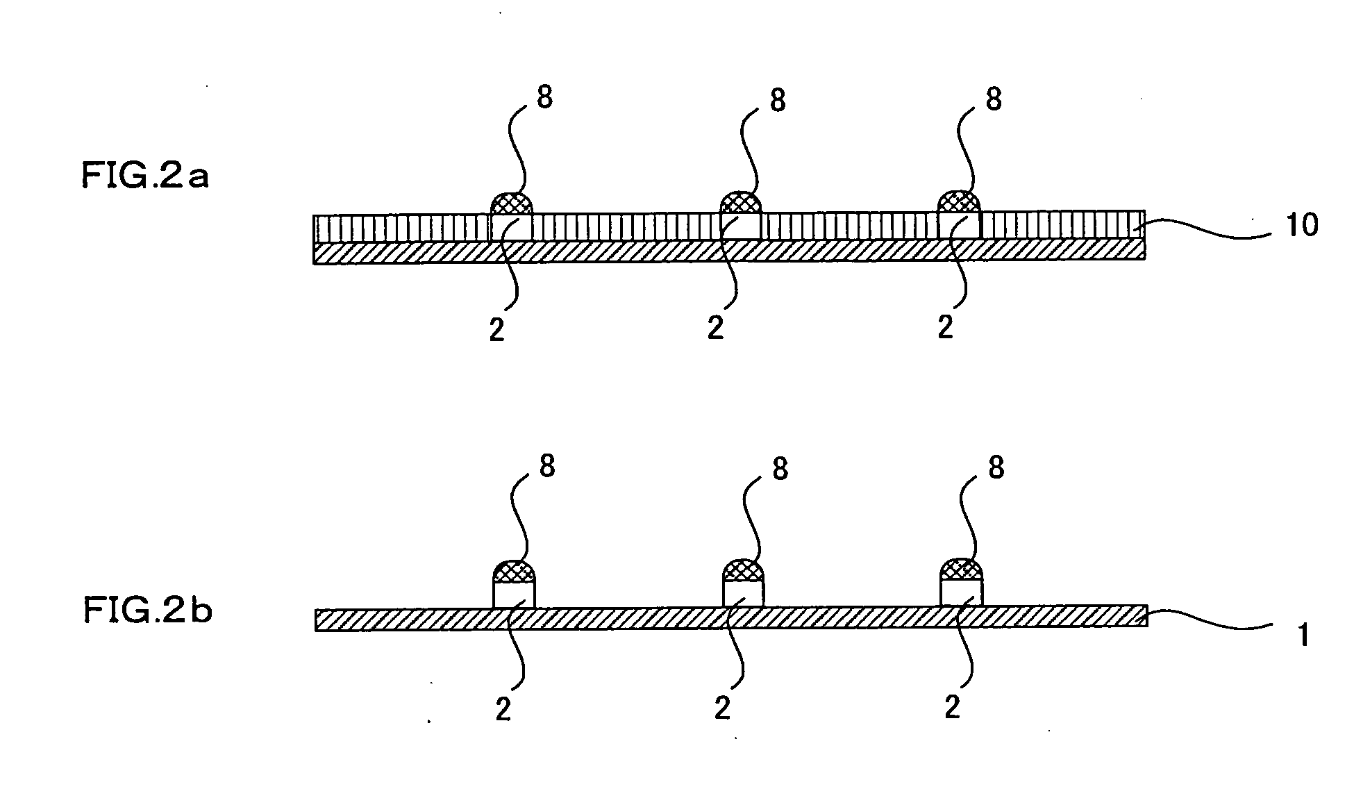
[0400] Next, the third embodiment of the conductive pattern forming body of the present invention will be explained. The third embodiment of the conductive pattern forming body of the present invention comprises: a base material; a photocatalyst treatment layer contains at least a photocatalyst, on the base material; a wettability variable layer whose wettability of an energy irradiated part is changed so as a contact angle to a liquid is reduced, on the photocataylst treatment layer; and a metal composition formed on the wettability variable layer by solidifying a metal colloid in a pattern.

[0401] The conductive pattern forming body of this embodiment is provided with the wettability variable layer, and it is therefore, possible to adhere the metal colloid in a pattern easily with high precision by utilizing a difference in lyophilic properties. Also, since the photocatalyst treatment layer and the conductive pattern are not directly in contact, the possibility ...


PUM

PropertyMeasurementUnit
contact angleaaaaaaaaaa

Abstract

It is a main object of the present invention to provide a method for manufacturing a conductive pattern capable of forming a highly precise pattern, also capable of forming by using a simple process, and being free from problems such as treatment of waste fluids. In order to attain the above object, the present invention provides a method for manufacturing a conductive pattern forming body comprising: a pattern forming body substrate preparing process of preparing pattern forming body substrate comprising a base material, and a photocatalyst containing layer formed on the base material comprising a photocatalyst and a binder whose wettability of an energy irradiated part is changed so as a contact angle to a liquid is reduced; a wettability pattern forming process of forming wettability pattern comprising a liquid repellent area and a lyophilic area on the photocatalyst containing layer by irradiating the photocatalyst containing layer in a pattern with energy; a metal colloid coating process of adhering a metal colloid only to the lyophilic area of the surface of the photocatalyst containing layer on which the wettability pattern is formed, by coating the metal colloid; and a conductive pattern forming process of forming conductive pattern by solidifying the metal colloid adhered to the lyophilic area of the wettability pattern.

Description

BACKGROUND OF THE INVENTION [0001] 1. Field of the Invention [0002] The present invention relates to a method for manufacturing a conductive pattern forming body which may be used in coatings such as various highly precise electric circuits such as a printed-circuit board. [0003] 2. Description of the Related Art [0004] Conventionally, when highly precise conductive pattern forming body such as a printed-circuit board is manufactured, a photoresist such as a dry film is laminated on a copper-clad laminate which is formed by plating the entire surface of a substrate with copper, followed by pattern-exposure using a photomask or the like and developing, thereby forming the conductive pattern forming body. [0005] However, in such a method using photolithography method, it is necessary to pass through various processes such as plating of a substrate with a metal, formation of a photoresist layer, exposure and developing, making the method for manufacturing complicated and a cost may be ...

Claims


Application Information

Patent Timeline
Patent Type & Authority Applications(United States)
IPC IPC(8): C23C18/12G03F7/004G03F7/075G03F7/40H05K3/12
CPCB82Y30/00C23C18/06C23C18/1216C23C18/14G03F7/0046H05K2203/1173G03F7/0757G03F7/405H05K3/1208H05K3/1241H05K2203/107G03F7/0047C23C18/143
Inventor KOBAYASHI, HIRONORI
Owner DAI NIPPON PRINTING CO LTD
Why Eureka
Try Eureka