Lateral heterojunction bipolar transistor and method of manufacture using selective epitaxial growth

a heterojunction bipolar transistor and selective epitaxial growth technology, applied in the field of semiconductor/solid-state device manufacturing, basic electric elements, electrical equipment, etc., can solve the problems of slow hbts, poor noise performance, inherently damaged compound semiconductive materials, etc., to reduce the load capacitance, reduce the parasitic capacitance, and reduce the collector-substrat capacitance. high

Active Publication Date: 2005-06-02
CHARTERED SEMICONDUCTOR MANUFACTURING
View PDF22 Cites 11 Cited by
  • Summary
  • Abstract
  • Description
  • Claims
  • Application Information

AI Technical Summary

Benefits of technology

[0016] Parasitic capacitances are reduced. There is a high reduction in the collector-substrate capacitance thereby reducing the load capacitance at high frequencies. There is a significant reduction in the base-collector capacitance because there is no extrinsic base directly contacting the collector.

Problems solved by technology

Several of these processing steps inherently damage the compound semiconductive material.
Etching polysilicon over a compound semiconductive layer, for example, adversely affects the compound semiconductive material because the etchants used do not selectively etch only the polysilicon.
Some of the compound semiconductive material is also etched during this processing step, resulting in HBTs that are slower and exhibit poor noise performance compared to other HBTs on the same semiconductor wafer.
The adverse effects of etching the emitter window persist however.
The lack of adequate controls and reproducibility of over-etching typically results in the intrinsic base being implanted after formation of the emitter window.
Implantation on the over-etched surface does not overcome the problems associated with the over-etched surface.
However, this technique has the problem of ion channeling, which limits the minimum thickness of the base layer.
Another disadvantage of ion implantation is that the compound semiconductive layer is often damaged by the ions during implantation.
This annealing step, however, alters the profile of concentration levels of the dopants within the various layers of semiconductive materials forming the transistor to create undesirable dopant profiles within the various material layers.
Existing methods of manufacturing HBTs still have the problems associated with over-etching, the detrimental effects of ion implantation and annealing, and consistency of manufacturability.
Furthermore, the differences in manufacturing techniques used to form complimentary metal oxide semiconductor (CMOS) transistors and HBTs have made it difficult to manufacture bipolar complimentary metal oxide semiconductor (BiCMOS) integrated circuits using compound semiconductive materials that have proven to be useful in HBTs.
Solutions to these problems have been long sought but prior developments have not taught or suggested any solutions and, thus, solutions to these problems have long eluded those skilled in the art.

Method used


Image

  • Lateral heterojunction bipolar transistor and method of manufacture using selective epitaxial growth
  • Lateral heterojunction bipolar transistor and method of manufacture using selective epitaxial growth
  • Lateral heterojunction bipolar transistor and method of manufacture using selective epitaxial growth

Examples


Embodiment Construction

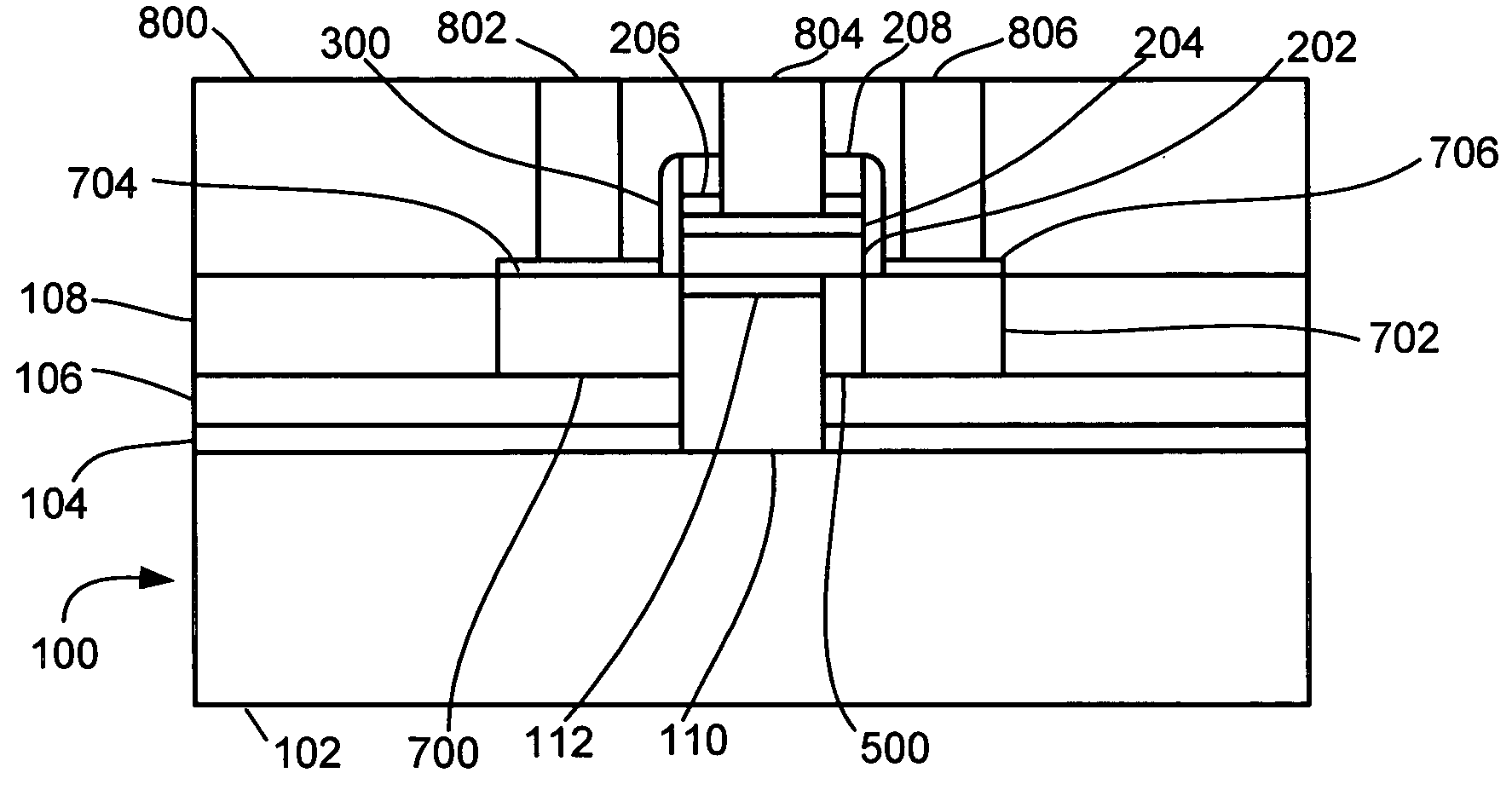
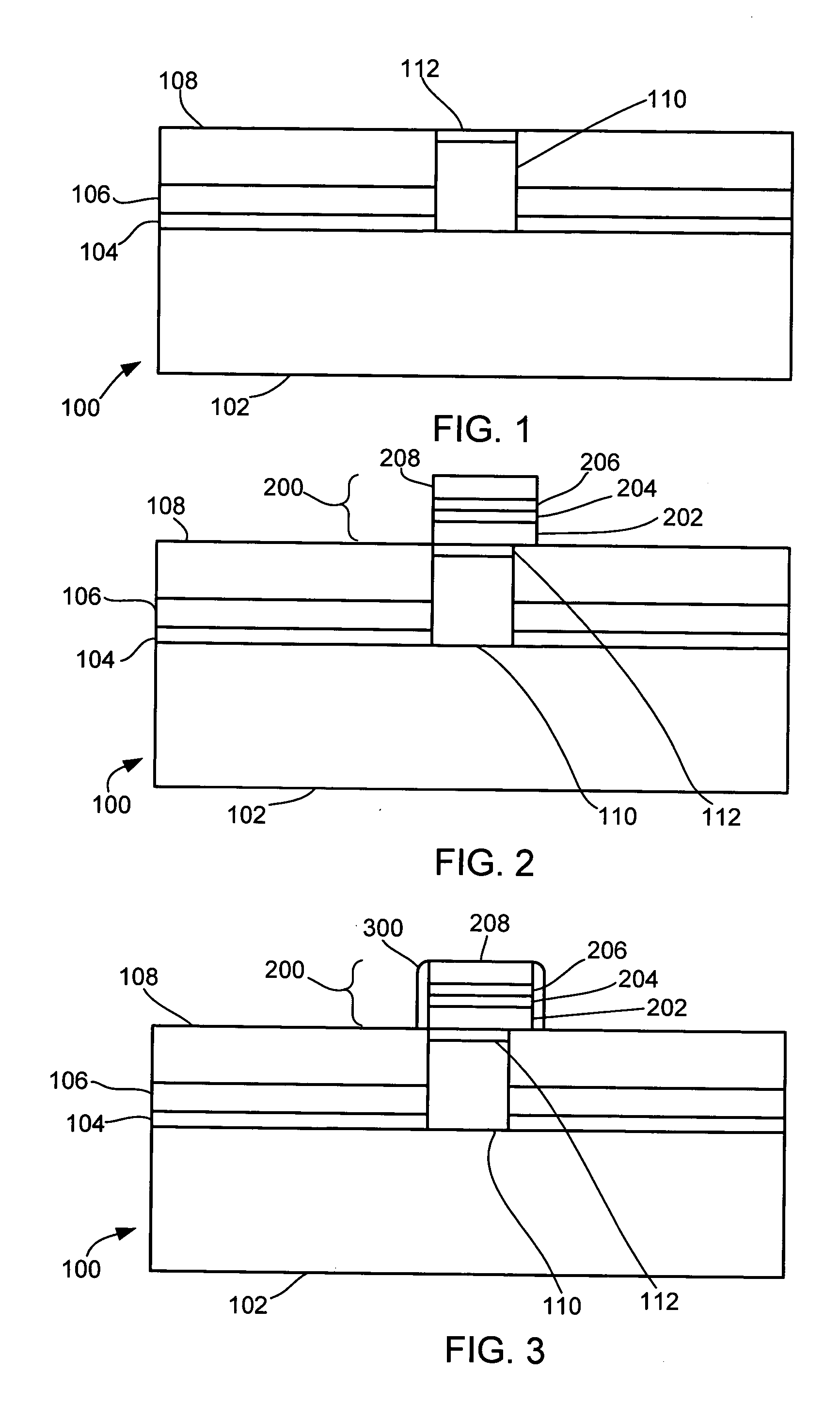
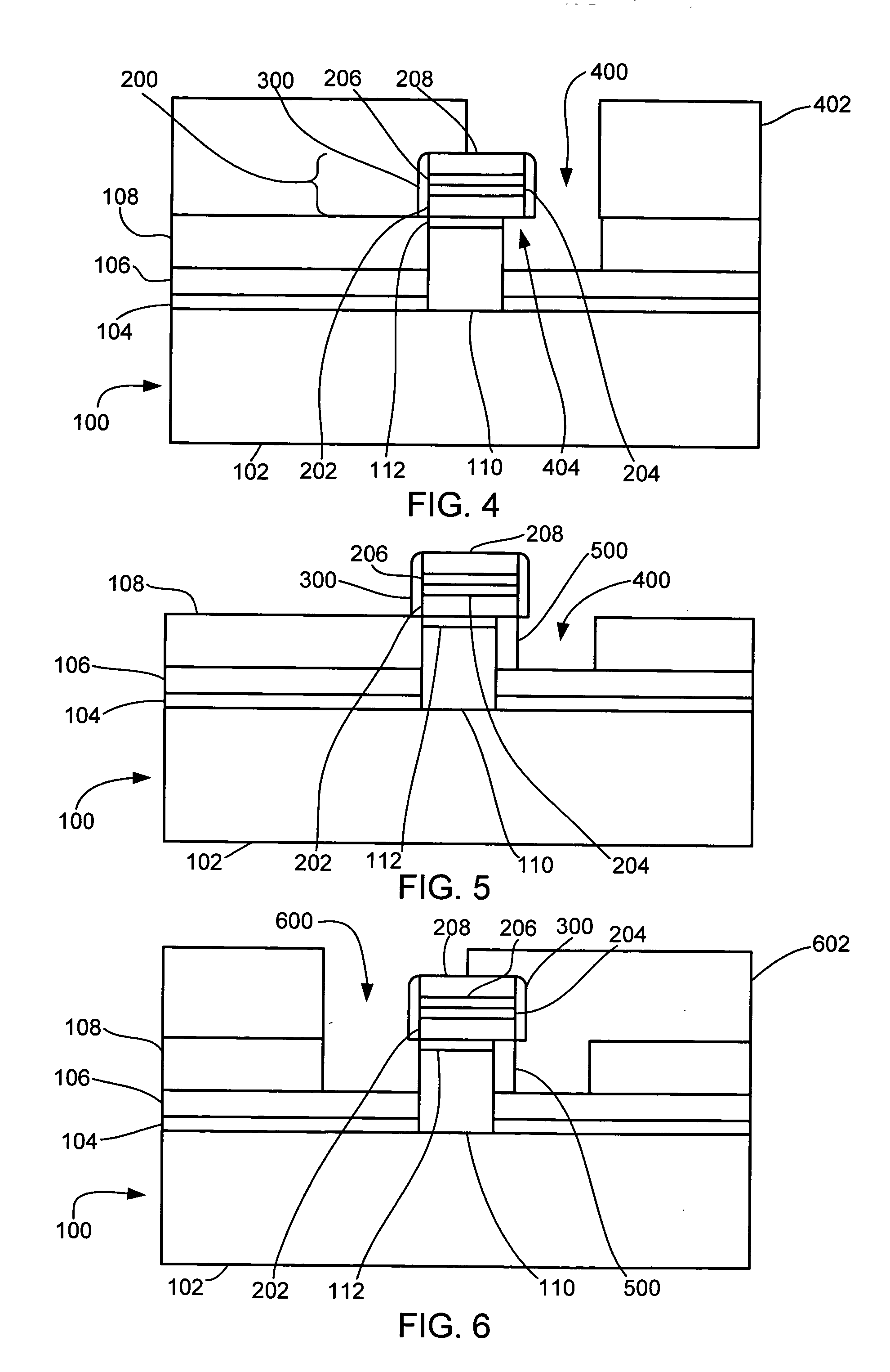
[0055] In the following description, numerous specific details are given to provide a thorough understanding of the invention. However, it will be apparent to one skilled in the art that the invention may be practiced without these specific details. In order to avoid obscuring the present invention, some well-known configurations and process steps are not disclosed in detail.

[0056] Likewise, the drawings showing embodiments of the apparatus are semi-diagrammatic and not to scale and, particularly, some of the dimensions are for the clarity of presentation and are shown greatly exaggerated in the FIGs. Generally, the device can be operated in any orientation.

[0057] The term “horizontal” as used herein is defined as a plane parallel to the conventional plane or surface of a semiconductor wafer or substrate, regardless of its orientation. The term “vertical” refers to a direction perpendicular to the horizontal as just defined. Terms, such as “on”, “above”, “below”, “bottom”, “top”, ...


PUM


Abstract

A method for manufacturing a heterojunction bipolar transistor is provided. An intrinsic collector structure is formed on a substrate. An extrinsic base structure partially overlaps the intrinsic collector structure. An intrinsic base structure is formed adjacent the intrinsic collector structure and under the extrinsic base structure. An emitter structure is formed adjacent the intrinsic base structure. An extrinsic collector structure is formed adjacent the intrinsic collector structure. A plurality of contacts is formed through an interlevel dielectric layer to the extrinsic collector structure, the extrinsic base structure, and the emitter structure.

Description

TECHNICAL FIELD [0001] The present invention relates generally to semiconductor technology, and more particularly to heterojunction bipolar transistors and a method of manufacturing therefor using selective epitaxial growth. BACKGROUND ART [0002] A popular device for controllably varying the magnitude of electrical current flowing between two terminals is a bipolar junction transistor (BJT). BJTs have three terminals. The three terminals include a base terminal, a collector terminal, and an emitter terminal. The movement of electrical charge carriers, which produce electrical current flow between the collector and the emitter terminals, varies dependent upon variations in the voltage on the base terminal thereby causing the magnitude of the current to vary. Thus, the voltage across the base and emitter terminals controls the current flow through the emitter and collector terminals. [0003] The terminals of a BJT are connected to their respective base, collector and emitter structures...

Claims


Application Information

Patent Timeline
Patent Type & Authority Applications(United States)
IPC IPC(8): H01L21/331H01L29/737
CPCH01L29/737H01L29/66242
Inventor VERMA, PURAKH RAJCHU, SHAO-FU SANFORDCHAN, LAPZHENG, JIA ZHENLI, JIAN XUN
Owner CHARTERED SEMICONDUCTOR MANUFACTURING
Why Eureka
Try Eureka