TFT array substrate and liquid crystal display device using it

a technology of array substrate and liquid crystal display device, which is applied in the direction of identification means, semiconductor devices, instruments, etc., can solve the problems of large variation in area, no consideration, and no disclosure, and achieve the effect of reducing the load capacitance of the gate line, reducing the uneven shot and flicker, and reducing the aperture ratio

Inactive Publication Date: 2006-08-29
TRIVALE TECH
View PDF10 Cites 5 Cited by
  • Summary
  • Abstract
  • Description
  • Claims
  • Application Information

AI Technical Summary

Benefits of technology

[0010]The present invention has been made to solve the above problems, and an object of the invention is to provide a TFT array substrate having a large aperture ratio in which the frequency of occurrence of display defects such as shot unevenness and a flicker due to alignment errors in a photolithography apparatus in an array substrate manufacturing process can be decreased and the load capacitance of the gate line can be reduced, as well as a liquid crystal display device using it.
[0018]Advantages of the invention will be described below. As described above, according to the invention, in a TFT array substrate comprising a plurality of gate lines formed on an insulative substrate, each of the gate lines including a gate electrode, a plurality of source lines crossing the gate lines, each of the source lines including a source electrode, a semiconductor layer formed on the gate electrode with a gate insulating film interposed in between, a thin-film transistor formed by the source electrode and a drain electrode, the source electrode and drain electrode are connected to the semiconductor layer, and a pixel electrode connected to a drain line extending from the drain electrode, the widths of crossing portions of the semiconductor layer and the drain line overlapping with it that cross an edge line of the gate electrode are made smaller than the width of the drain electrode that is equal to a channel width of the thin-film transistor. Therefore, differences in the overlap area of the gate electrode and the drain electrode between shots that occur due to alignment errors in a photolithography apparatus used in patterning the gate electrodes, the drain electrodes, and the source electrodes become small, whereby the variation of the parasitic capacitance which is a parameter representing the feedthrough voltage can be reduced and hence the frequency of occurrence of display defects such as shot unevenness and a flicker can be decreased.
[0019]Further, the drain electrode and the drain line have a portions that are located over the gate electrode and do not coextend with the semiconductor layer. Therefore, the area of the semiconductor layer that is located outside the drain electrode and the drain line becomes small and the capacitance formed by the gate electrode and the portion of the semiconductor layer that is located outside the drain electrode becomes small and hence has almost no influence on the feedthrough voltage. Therefore, the frequency of occurrence of display defects such as shot unevenness and a flicker can further be decreased. Still further, the invention can make the load capacitance of the gate line smaller than in the conventional TFT structure. In addition, employment of the pixel line makes it possible to provide a TFT array substrate having a larger aperture ratio than conventional ones do, as well as a liquid crystal display device having superior display characteristics.

Problems solved by technology

However, there is a problem that no consideration is given to alignment errors in the direction perpendicular to the channel width 11 and such alignment errors cause large variations in areas.
However, this publication has no disclosure relating to the width of a semiconductor layer on the step portion.

Method used


Image

  • TFT array substrate and liquid crystal display device using it
  • TFT array substrate and liquid crystal display device using it
  • TFT array substrate and liquid crystal display device using it

Examples


embodiment 1

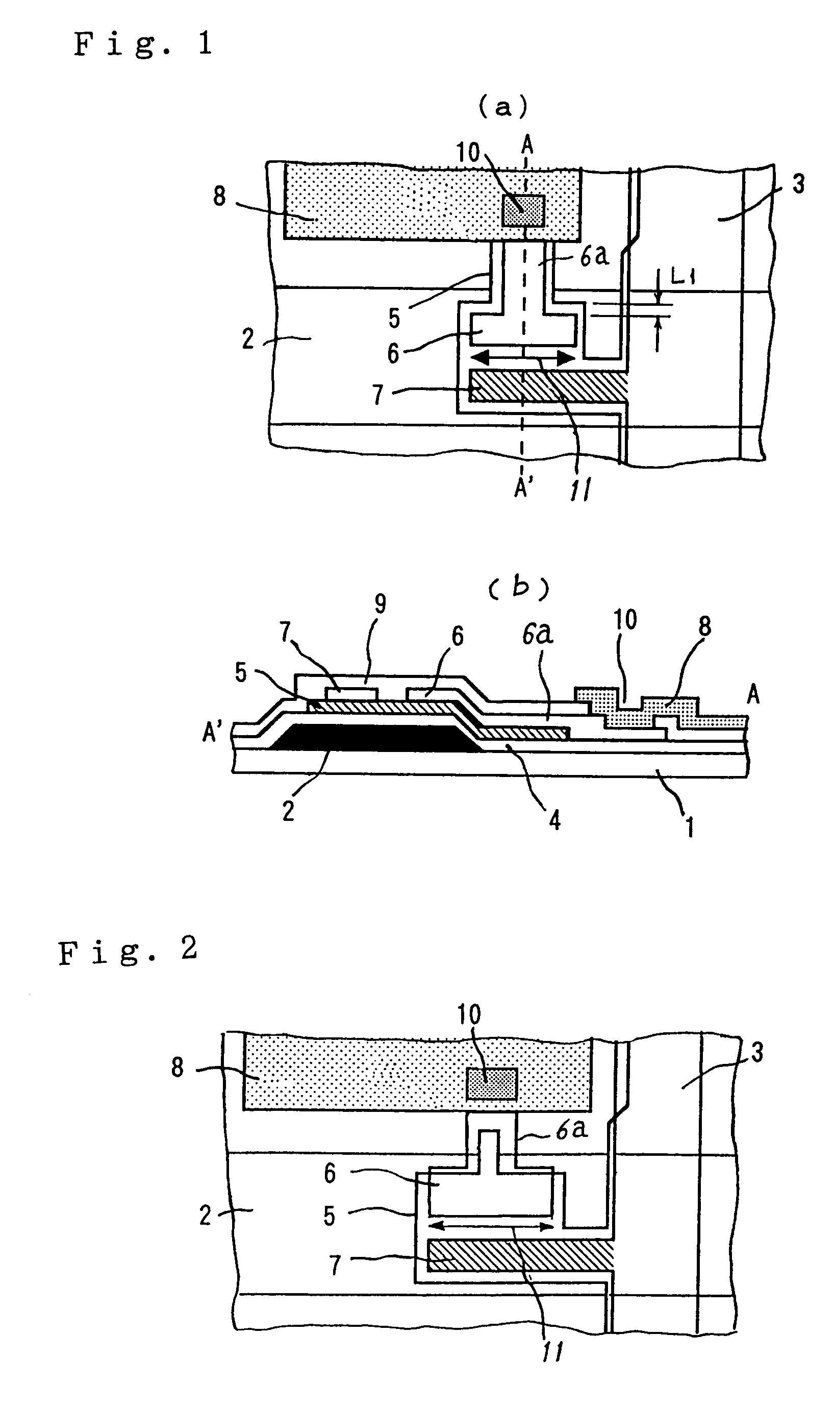
[0028]Embodiments of the present invention will be hereinafter described with reference to the drawings. FIG. 1(a) is a plan view showing a TFT portion as a switching element of a TFT array substrate according to a first embodiment of the invention, and FIG. 1(b) is a sectional view taken along line A–A′ in FIG. 1(a).

[0029]In the figures, reference numeral 1 denotes a transparent insulative substrate; 2, a plurality of gate lines formed on the transparent insulative substrate 1 and gate electrodes provided in the gate lines; and 3, a plurality of source lines that have source electrodes 7 and cross the gate lines 2. Reference numeral 5 denotes a semiconductor layer formed on each gate electrode 2 with a gate insulating film 4 interposed in between. A source electrode 7 and a drain electrode 6 that are connected to the semiconductor layer 5 constitute a TFT. Reference numeral 8 denotes a pixel electrode that is a transparent conductive film and is connected to a drain line 6a extendi...

embodiment 2

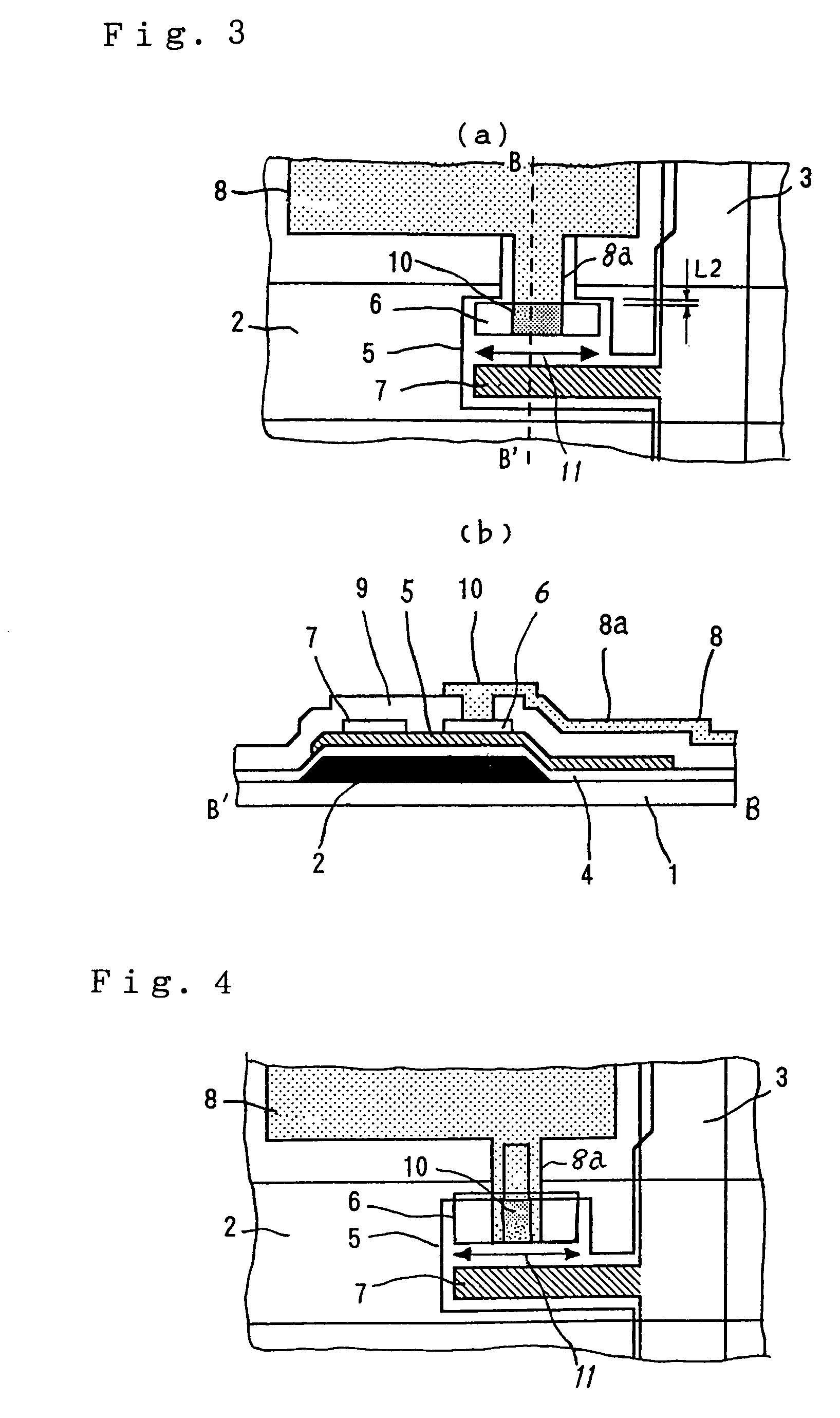
[0035]FIG. 2 is a plan view showing a TFT portion as a switching element of a TFT array substrate according to a second embodiment of the invention. The same or corresponding parts are given the same symbols in the figure and will not be described.

[0036]In this embodiment, as same as the first embodiment, the widths of those crossing portions of the semiconductor layer 5 and the drain line 6a overlapping with it which cross the edge line of the gate electrode 2 are made smaller than the width of the drain electrode 6 that is equal to the channel width 11 of the TFT. In addition, the drain electrode 6 and the drain line 6a have portions that are located over the gate electrode 2 and do not coextend with the semiconductor layer 5. With this measure, the area of the portion of the semiconductor layer 5 that is located over the gate electrode 2 and is located outside the drain electrode 6 is made smaller than in the first embodiment.

[0037]In the above-described TFT structure according t...

embodiment 3

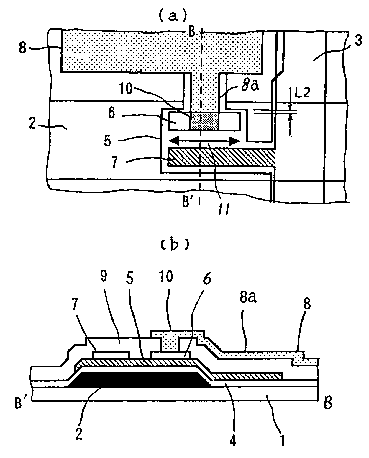
[0039]FIG. 3(a) is a plan view showing a TFT portion as a switching element of a TFT array substrate according to a third embodiment of the invention, and FIG. 3 (b) is a sectional view taken along line B–B′ in FIG. 3(a). In the figures, reference symbol 8a denotes a pixel line that extends from the pixel electrode 8 and is connected to the drain electrode 6. In the figures, the same or corresponding parts are given the same symbols. The manufacturing method of the TFT array substrate according to this embodiment is approximately the same as in the first embodiment except that pixel electrodes 8 having pixel lines 8a are patterned and the pixel lines 8a are connected to drain electrodes 6 through contact holes 10, and hence will not be described.

[0040]In this embodiment, in the TFT array substrate in which the drain electrode 6 of the TFT is formed on the semiconductor layer 5 that is formed on the gate electrode 2, the contact hole 10 is formed above the drain electrode 6, and the ...


PUM

PropertyMeasurementUnit
distanceaaaaaaaaaa
feedthrough voltageaaaaaaaaaa
widthaaaaaaaaaa

Abstract

The widths of those portions of a semiconductor layer 5 and a drain line 6a overlapping with it which cross an edge line of a gate electrode 2 are made smaller than the channel width of a thin-film transistor. With this measure, the overlap area of the gate electrode 2 and a drain electrode 6 is reduced. As a result, a variation of the above overlap area due to alignment errors in a photolithography apparatus used in patterning the gate lines 2, the drain electrodes 6, and source electrodes 7 can be reduced and the frequency of occurrence of display defects can be decreased.

Description

[0001]This application is a divisional of application Ser. No. 10 / 049,715 filed Feb. 14, 2002, now U.S. Pat. No. 6,825,907 which is a 371 application of PCT / JP01 / 04885 filed Jun. 11, 2001.TECHNICAL FIELD[0002]The present invention relates to an active matrix TFT array substrate incorporating thin-film transistors (hereinafter referred to as “TFTs”) as switching elements as well as to a liquid crystal display device using it.BACKGROUND ART[0003]FIG. 7(a) is a plan view showing one pixel of a conventional TFT array substrate, FIG. 7(b) is a plan view showing a TFT portion as a switching element, and FIG. 7(c) is a sectional view taken along line D–D′ in FIG. 7(b). In the figures, reference numeral 1 denotes a transparent insulative substrate; 2, a plurality of gate lines formed on the transparent insulative substrate 1 and gate electrodes provided in the gate lines; 3, a plurality of source lines that have source electrodes 7 and cross the gate lines 2; and 5, a semiconductor layer fo...

Claims


Application Information

Patent Timeline
Patent Type & Authority Patents(United States)
IPC IPC(8): G02F1/136G02F1/1343G02F1/1368G09F9/30H01L27/12H01L29/423H01L29/786
CPCH01L29/42384H01L27/12G02F1/1368G02F1/136
Inventor HASHIGUCHI, TAKAFUMIYAMAGUCHI, TAKEHISANAKAGAWA, NAOKI
Owner TRIVALE TECH
Why Eureka
Try Eureka