Light emitting device

a technology of light emitting device and light source, which is applied in the direction of semiconductor devices, basic electric elements, electrical apparatus, etc., can solve the problems of increasing manufacturing cost, complicated structure, and complicated structure of gan-based led, and achieves simple structure, high emission efficiency, and easy manufacturing

Inactive Publication Date: 2006-07-20
SUMITOMO ELECTRIC IND LTD
View PDF3 Cites 64 Cited by
  • Summary
  • Abstract
  • Description
  • Claims
  • Application Information

AI Technical Summary

Benefits of technology

[0018] An object of the present invention is to provide a light emitting device having a simple structure and hence allowing easy manufacturing, assuring high emission efficiency stably for a long period of time.
[0020] In this arrangement, the n-type electrode is provided on the back surface (second main surface) of the nitride semiconductor substrate having low electrical resistance, and therefore, even when the n-electrode is formed with small coverage ratio or large aperture ratio, it is possible to cause current to flow uniformly and entirely through the nitride semiconductor substrate. Therefore, the ratio of light absorbed at the emitting surface can be reduced and light emission efficiency can be increased. Needless to say, the light may be emitted not only from the second main surface but also from side surfaces. This is the same in the light emitting devices described in the following.
[0022] As the GaN substrate has superior conductivity, a protection circuit against surge voltage becomes unnecessary, and superior withstanding characteristic can be attained.
[0023] Complicated process steps are not involved, and therefore, manufacturing cost can easily be reduced.
[0024] Further, trenches are formed on the second main surface as the light emitting surface of the nitride semiconductor substrate, and therefore light can be taken out also from the side surfaces of the trenches. As a result, efficiency of use of light from the light emitting device can be improved.

Problems solved by technology

The structure of GaN-based LED is very complicated, as can be seen from FIG. 70.
In the GaN-based LED using a sapphire substrate shown in FIG. 70 described above, the structure becomes complicated, inherently increasing the manufacturing cost.
Therefore, such a complicated structure is undesirable.
Such increase in area is limited in the structure shown in FIG. 70, and hence, the optical output is also limited.
Further, from the viewpoint of releasing heat generated by the current, arrangement of two electrodes on one surface is undesirable.
Further, a current flowing through n-type GaN layer 102 in a direction parallel to the substrate meets much resistance, resulting in heat generation and increased driving voltage and hence increased power consumption.
Particularly, when the n-type GaN layer is made thin to make shorter the step of film formation, production yield of exposure of the n-type GaN film significantly decreases, in addition to the above-described problems of heat generation and increased power consumption.
Light emitting devices including the above-described device using a sapphire substrate generally have limited area of heat radiation, and have large thermal resistance (increase in temperature caused by unit energy input per unit area), and therefore, it is impossible to inject a large current per one light emitting device.
Further, in the GaN-based LED using the sapphire substrate, area for heat radiation is limited, and therefore, it becomes unavoidable to adopt a structure in which p- and n-electrodes are formed in a shape of a comb to increase the area of contact, so as to reduce electrical resistance as much as possible and to reduce heat generation.
Processing of such a comb-shaped electrode is difficult and leads to an increased manufacturing cost.
This leads to lower light emission efficiency at the main surface of sapphire substrate.
Though light emission efficiency is important, there is a still more problem.
Sealing resin positioned at the side portion and irradiated with the light beams is damaged, making shorter the life of the light emitting device.
Therefore, light emission cannot fully be activated in the quantum well structure, resulting in lower optical output.
Further, electrical resistance increases, causing the problems of heat generation and electrical capacitance.

Method used


Image

  • Light emitting device
  • Light emitting device
  • Light emitting device

Examples


embodiment 1

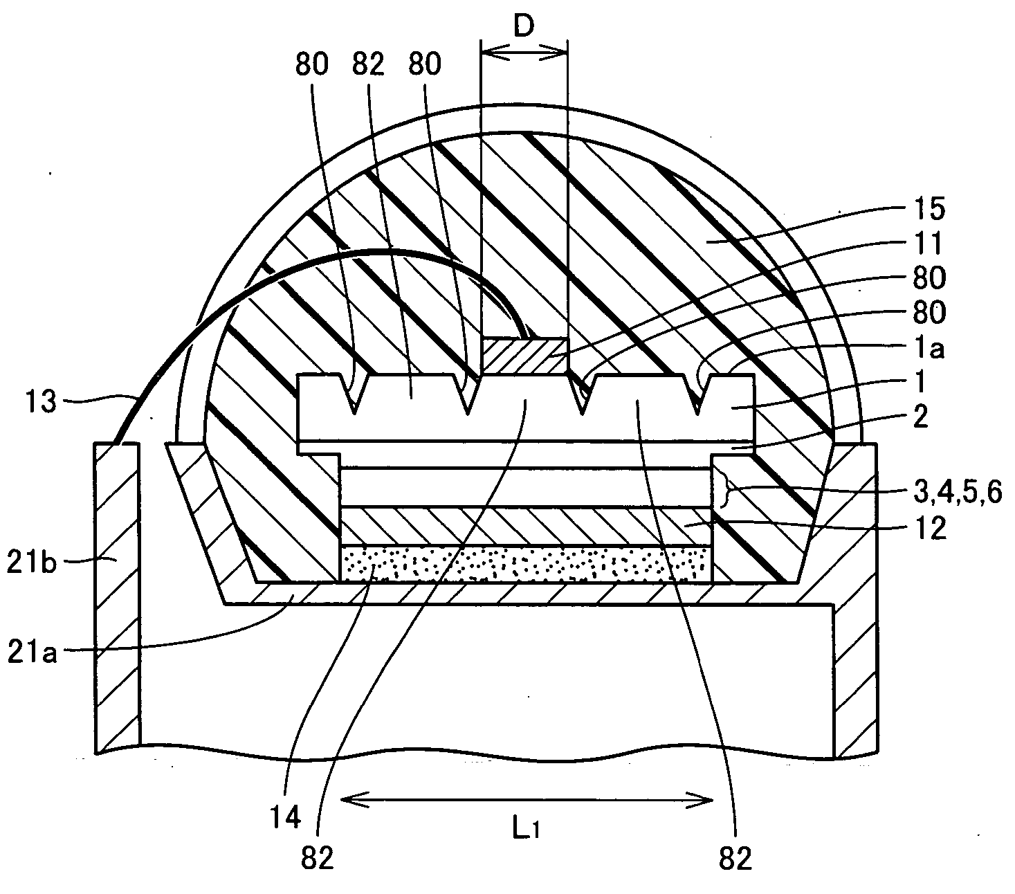
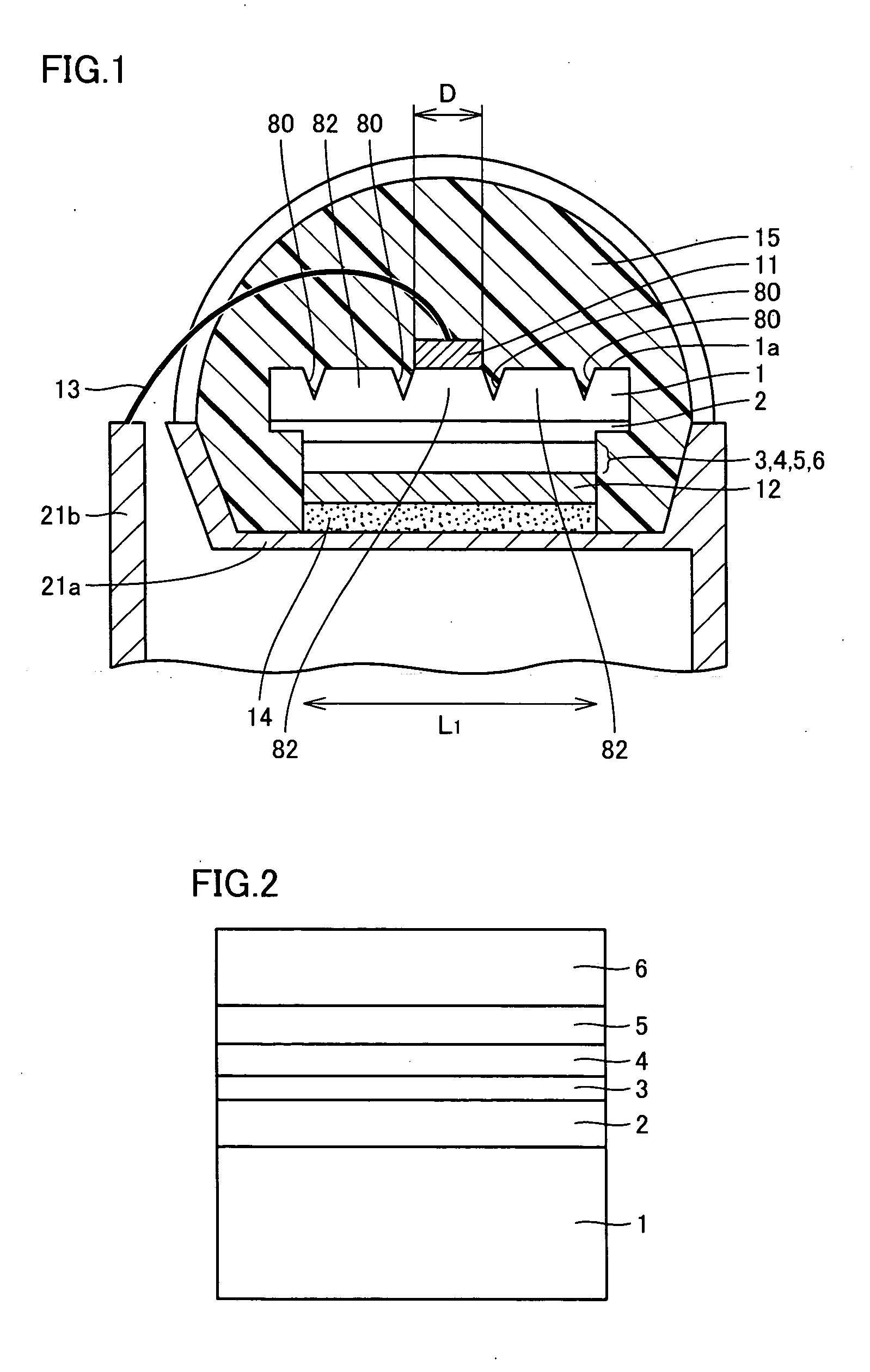
[0118] First, a sapphire substrate and the GaN substrate as the nitride semiconductor substrate will be compared. Here, an LED as Example A of Embodiment 1 of the present invention has the same structure as the LED shown in FIG. 1. In the following, the LED of Example A will be described with reference to FIG. 1. As shown in FIG. 1, the LED of Example A has a stacked structure, which will be described in detail later, including a light generating layer and the like formed on the side of the first main surface of GaN substrate 1, and p-electrode 12 is provided. One characteristic of the present invention is that p-electrode 12 is mounted face-down on lead frame mounting portion 21a by conductive adhesive 14.

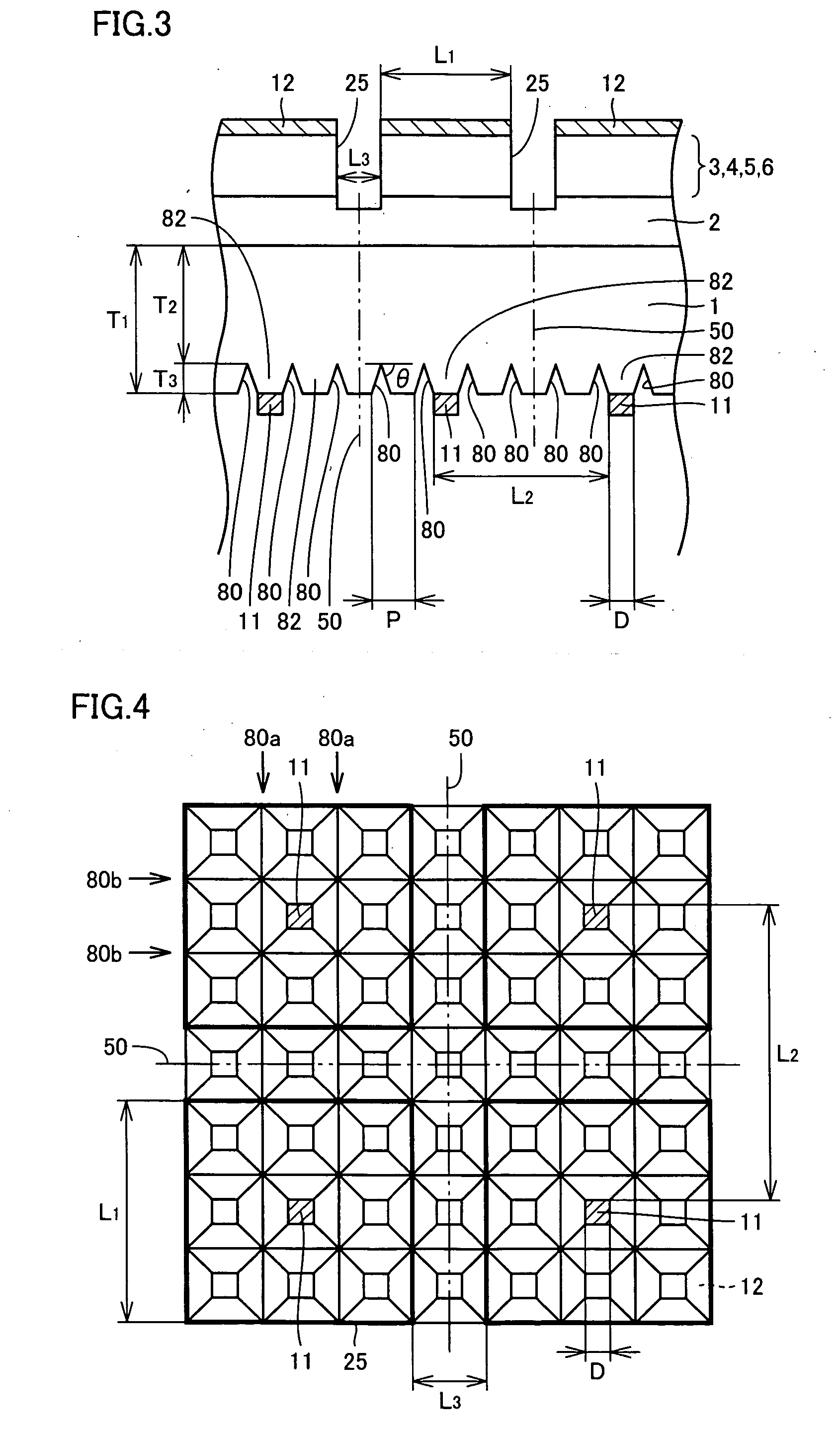
[0119] The second main surface 1a of GaN substrate 1 is a light emitting surface that emits light generated in the light generating layer, and an n-electrode 11 is formed on this surface. A plurality of trenches 80 extending in directions vertical to and parallel to the surface o...

embodiment 2

[0153] In Embodiment 2, Example C of the present invention having a larger area will be described. Example C of the present invention has the same structure as Example A shown in FIG. 1, except that the length L1, which is 0.3 mm (300 μm) in Example A, is made 3 mm in Example C, that is, ten times larger than Example A. Accordingly, the area is 100 times larger. The method of manufacturing Example C is as follows.

example c

[0154] (c1) to (c5) Process steps corresponding to those of Example A of the present invention are performed, except that a large GaN substrate is used.

[0155] (c6) On the second main surface as the back surface of GaN substrate, n-electrodes having a square two-dimensional shape, with the width D of each side being 100 μm, were formed each at the center of the chip, apart by 3.1 mm, by photolithography, vapor deposition and lift-off method. As the n-electrode, a stacked structure including (Ti layer of 20 nm / Al layer of 100 nm / Ti layer of 20 nm / Au layer Of 200 nm) in this order from the lower side was formed in contact with the back surface of the GaN substrate. The resulting body then was heated in an inert atmosphere, so that contact resistance was made to be at most 1E-5 Ω·cm 2.

[0156] (c7) and (c8) Process steps corresponding to those of Example A of the present invention were performed.

[0157] (c9) Thereafter, scribing was performed to attain a prescribed shape, and the result...


PUM


Abstract

A light emitting device having a simple structure that can be easily manufactured, attaining high light emitting efficiency stably for a long time is obtained, which light emitting device includes: a GaN substrate as a nitride semiconductor substrate and, on a first main surface of the nitride semiconductor substrate, an n-type AlxGa1-xN layer, a p-type AlxGa1-xN layer positioned further than the n-type AlxGa1-xN layer viewed from the nitride semiconductor substrate, and a quantum well positioned between the n-type AlxGa1-xN layer and the p-type AlxGa1-xN layer. In the light emitting device, specific resistance of the nitride semiconductor substrate is at most 0.5 Ω·cm, the side of p-type AlxGa1-xN layer is mounted face-down, and the light is emitted from the second main surface 1a that is opposite to the first main surface of the nitride semiconductor substrate. The second main surface 1a of nitride semiconductor substrate has trenches formed therein.

Description

BACKGROUND OF THE INVENTION [0001] 1. Field of the Invention [0002] The present invention relates to a light emitting device and, more specifically, to a light emitting device formed of a nitride semiconductor. The light emitting device in accordance with the present invention may simply refer to a semiconductor device or a semiconductor chip mainly formed of a nitride semiconductor substrate and a semiconductor layer stacked thereon, or a device having the semiconductor chip mounted on a mounting component and resin-sealed. The term may also refer to both types of devices. The semiconductor chip may be simply referred to as a chip. Further, of the chip, the substrate and an epitaxial layer formed thereon may simply be referred to as a substrate. [0003] 2. Description of the Background Art [0004] A white light emitting diode (LED) is at present popularly used for illumination for small electronic equipment such as a portable information terminal, and it will possibly be used for ill...

Claims


Application Information

Patent Timeline
Patent Type & Authority Applications(United States)
IPC IPC(8): H01L33/00H01L33/06H01L33/32H01L33/38H01L33/40H01L33/56H01L33/60H01L33/62
CPCH01L33/025H01L33/22H01L2224/45139H01L2224/45144H01L2924/00H01L2224/48091H01L2224/48247H01L2924/00014H01L2924/10253H01L2924/3025H01L2224/45015H01L2224/73265H01L2224/8592H01L2924/00011H01L2924/10155H01L2924/10158H01L2924/20752H01L2924/2076H01L2924/01049H01L2924/01004H01L2924/01005
Inventor NAGAI, YOUICHIKITABAYASHI, HIROYUKISAITO, HIROHISAIKEDA, AYAKO
Owner SUMITOMO ELECTRIC IND LTD
Why Eureka
Try Eureka