Semiconductor device

a technology of semiconductors and devices, applied in memory systems, transistors, instruments, etc., can solve the problems of high power consumption and different power consumption of high-capacity memory, and achieve the effects of reducing load capacitance of bit lines in memory arrays, suppressing power consumption, and increasing memory capacity

Inactive Publication Date: 2010-03-09
SEMICON ENERGY LAB CO LTD
View PDF17 Cites 5 Cited by
  • Summary
  • Abstract
  • Description
  • Claims
  • Application Information

AI Technical Summary

Benefits of technology

[0004]In order to provide a high-performance semiconductor device with low power consumption, it is necessary to realize a high-capacity memory with low power consumption. However, a high-capacity memory generally has high power consumption. In other words, there is a trade-off between performance and power consumption in a semiconductor device mounted with a memory. Also, in a high-capacity memory, power consumption differs depending on a physical address of a memory cell to be read from or written to. Therefore, in consideration of the maximum power consumption of a memory, it is necessary to provide measures for power source allotment and heat dissipation in designing a semiconductor device mounted with a memory. Accordingly, in order to provide a high-performance semiconductor device with low power consumption, it is necessary to mount a high-capacity memory with which power consumption can be reduced as well as with which power consumption can be made to be constant throughout the memory.
[0005]The present invention is made in view of the above problems, and a memory mounted to a semiconductor device includes a plurality of memory blocks, each including memory cells arranged in a matrix form. Note that the plurality of memory blocks included in the memory are arranged to be symmetrical. By arranging them in this manner, a wiring length of a bit line in a memory array can be shortened, and current consumption can be made to be even among data reading or writing from / to memory cells of a variety of addresses within the memory, at the same time as reducing load capacitance.
[0006]Also, a memory block including a memory cell to be read from or written to can be specified by a combination of some potentials among a plurality of address signals supplied to the memory. In such a memory, by the combination of the potentials of the address signals that can specify the memory block, at least one of address signals, reading control signals, writing control signals, and writing data signals supplied to memory blocks other than the above memory block has a constant value that is not dependent on a value of address signals, reading control signals, writing control signals, and writing data signals supplied to the memory. Accordingly, power consumption by a memory block that is irrelevant to data reading or writing can be reduced.
[0008]Also, in the first to n-th tiers, each memory block including a memory cell from / to which data reading or writing is carried out can be specified by a combination of some potentials among a plurality of address signals supplied to the memory. In such a memory, in the first to n-th tiers, by the combination of the potentials of the address signals that can specify the memory block in each of the first to n-th tiers, at least one of address signals, reading control signals, writing control signals, and writing data signals supplied to memory blocks other than the memory block in the first to n-th tiers has a constant value that is not dependent on a value of address signals, reading control signals, writing control signals, and writing data signals supplied to the memory. Accordingly, power consumption by a memory block that is irrelevant to data reading or writing can be reduced.
[0009]With a structure such as the foregoing, a high-performance and low and even power consumption semiconductor device including a high-capacity memory that has low and even power consumption can be provided.
[0027]By the present invention, since a memory can be divided into a plurality of memory blocks and memory blocks other than that which includes a memory cell to be read from or written to can be in a waiting state, power consumption can be suppressed even if capacity of the memory is increased. Further, by dividing the memory into a plurality of memory blocks and arranging the memory blocks to be symmetrical to each other, load capacitance of a bit line in a memory array can be reduced, and power consumption can be made to be even among data reading or writing from / to memory cells of a variety of addresses within the memory. In other words, a high-performance and low power consumption semiconductor device including a high-capacity memory, that has low and even power consumption can be provided.

Problems solved by technology

However, a high-capacity memory generally has high power consumption.
In other words, there is a trade-off between performance and power consumption in a semiconductor device mounted with a memory.
Also, in a high-capacity memory, power consumption differs depending on a physical address of a memory cell to be read from or written to.

Method used


Image

  • Semiconductor device
  • Semiconductor device
  • Semiconductor device

Examples


embodiment mode 1

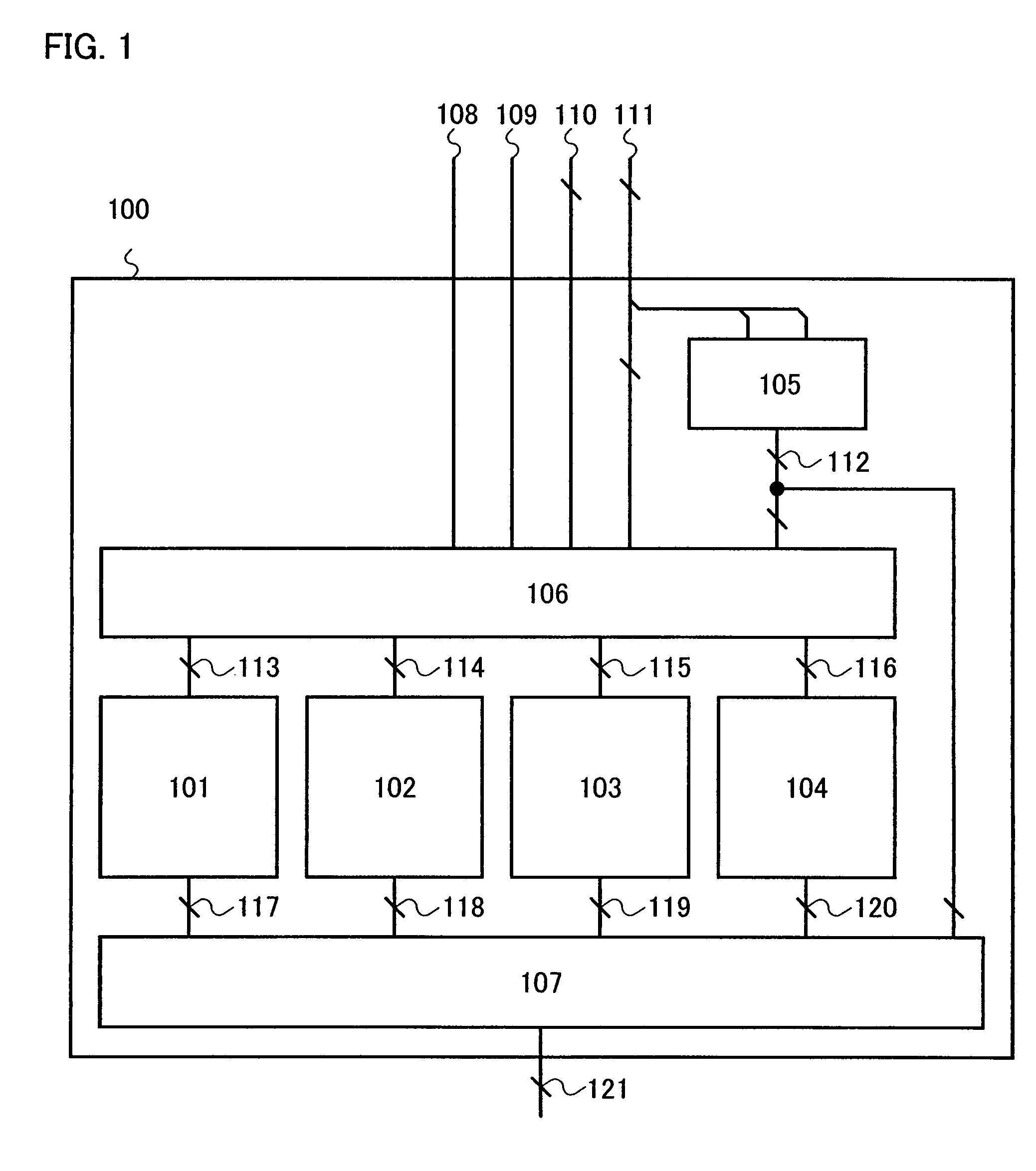
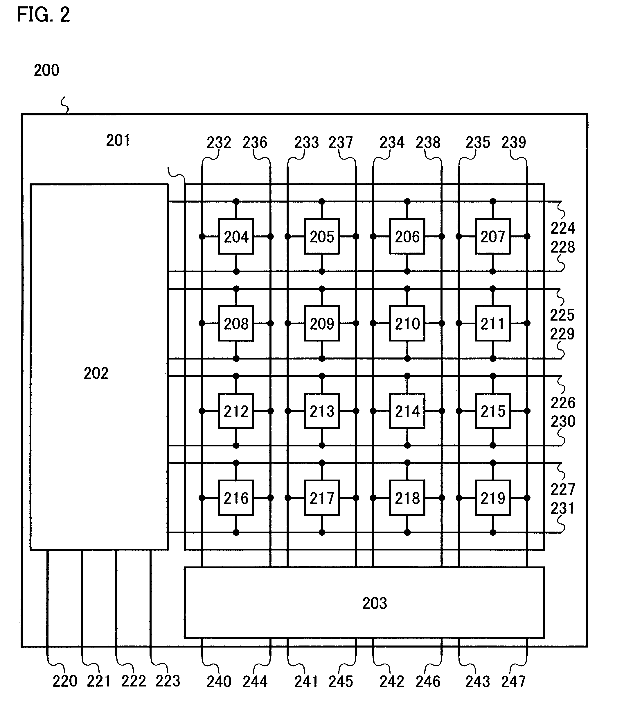
[0057]A first embodiment mode of a memory mounted to a semiconductor device of the present invention is described with reference to FIGS. 1 to 4. FIG. 1 is a block diagram of a memory of this embodiment mode; FIG. 2 is a block diagram of a memory block included in the memory of this embodiment mode; FIG. 3 is a timing chart of the memory block included in the memory of this embodiment mode; and FIG. 4 is a timing chart of the memory of this embodiment mode.

[0058]As shown in FIG. 1, a memory 100 of this embodiment mode includes first to fourth memory blocks 101 to 104, an operation control circuit 105, an input signal control circuit 106, and an output signal control circuit 107. Note that each of the first to fourth memory blocks 101 to 104 is a memory block 200 in FIG. 2.

[0059]Note that in this embodiment mode, a case of a memory including four memory blocks is described, in which a memory address signal is 4 bits, that is, 16 words, and a memory reading / writing data signal is 4 bi...

embodiment mode 2

[0105]As a second embodiment mode of a memory mounted to a semiconductor device in the present invention, a memory having a hierarchical structure is described with reference to FIGS. 2, 3, and 5 to 8. FIG. 2 is a block diagram of a memory block also used in the description of Embodiment Mode 1, and is a block diagram of a first-tier memory block in this embodiment mode. FIG. 3 is a timing chart of a memory block also used in the description of Embodiment Mode 1, and is a timing chart of the first-tier memory block in this embodiment mode. FIG. 5 is a block diagram of a memory block included in a memory in this embodiment mode, and is a block diagram of a second-tier memory block. FIG. 6 is a block diagram of a memory in this embodiment mode. FIG. 7 is a timing chart of the second-tier memory block in this embodiment mode. FIG. 8 is a timing chart of a memory in this embodiment mode.

[0106]In this embodiment mode, a case of a memory with a memory address signal of 6 bits, that is, 64...

embodiment 1

[0151]In this embodiment, an example of a memory mounted to a semiconductor device of the present invention is described with reference to FIGS. 9A to 9D. FIGS. 9A and 9B are examples of a memory cell and a row RW circuit, respectively, in a case where the memory mounted to the semiconductor device of the present invention is an SRAM (Static RAM). Also, FIGS. 9C and 9D are examples of a memory cell and a row RW circuit, respectively, in a case where the memory mounted to the semiconductor device of the present invention is a mask ROM.

[0152]First, a case where a memory of the present invention includes the memory cell in FIG. 9A and the row RW circuit in FIG. 9B is described.

[0153]In FIG. 9A, the memory cell includes a word signal line 901, first and second bit signal lines 902 and 903, first and second switch transistors 904 and 905, and first and second inverters 906 and 907. A gate electrode of each of the first and second switch transistors 904 and 905 is electrically connected t...


PUM


Abstract

An object is to realize high-capacity of a memory while reducing power consumption and making the power consumption even throughout the memory. A memory includes a plurality of memory block arranged to be symmetrically to each other. Also, a specific combination of signals among address signals supplied to the memory, a memory block including a memory cell to be read from or written to is specified. Further, signals supplied to other memory blocks than the above memory block is maintained at a constant value. Consequently, a wiring length of a bit line in a memory array can be shortened, and current consumption can be made to be even among data reading or writing from / to memory cells of a variety of addresses within the memory, at the same time as reducing load capacitance.

Description

TECHNICAL FIELD[0001]The present invention relates to a semiconductor device. In particular, the present invention relates to a semiconductor device mounted with a memory.BACKGROUND ART[0002]In a semiconductor device mounted with a memory, the performance of the memory is extremely important in determining the performance of the semiconductor device. For example, in a semiconductor device mounted with a CPU and a memory, commands to be processed by the CPU and data necessary for the processing need to be stored in the memory. Also, processing by the CPU is progressed by sequential reading of the data in the memory. In other words, in a semiconductor device mounted with a CPU and a memory, in order to achieve higher performance, the CPU needs to be able to handle more complicated processes, and this calls for a high-capacity memory. Furthermore, in a semiconductor device mounted with a memory, the power consumption of the memory accounts for a large share of the power consumption of ...

Claims


Application Information

Patent Timeline
Patent Type & Authority Patents(United States)
IPC IPC(8): G11C8/00
CPCG11C5/02G11C5/04H01L27/12H01L21/84H01L27/1108G11C17/12H10B10/125G11C8/12G11C7/10
Inventor KUROKAWA, YOSHIYUKI
Owner SEMICON ENERGY LAB CO LTD
Why Eureka
Try Eureka