Light-emitting device, manufacturing method thereof, and electronic apparatus

a technology of light-emitting devices and manufacturing methods, which is applied in the direction of identification means, instruments, discharge tubes, etc., can solve the problems of reducing light-emitting efficiency, affecting the brightness of light-emitting elements, and not obtaining sufficient transmittance, etc., and achieves high reliability, high brightness, and high brightness.

Active Publication Date: 2005-06-02
SEIKO EPSON CORP
View PDF23 Cites 108 Cited by
  • Summary
  • Abstract
  • Description
  • Claims
  • Application Information

AI Technical Summary

Benefits of technology

[0071] Therefore, according to the present invention, since the electronic apparatus uses the light-emitting device described above as a display unit, the electronic apparatus comprises the display unit which can display bright image with high quality, high reliability, hig

Problems solved by technology

However, when such the construction is adopted, a transparent conductive film, typified by an ITO film, has high resistance as compared with a metallic film, typified by an Al film, and thus brightness irregularity of the light-emitting element is caused by a voltage drop due to the resistance of the transparent conductive film itself.
Further, if the upper electrode is formed with a metallic film such as Al, there is a problem in that sufficient transmittance is not obtained and the light emission efficiency is lowered.
Further, in almost all top-emission-type structures, the electrode is transparent, and thus sufficient transmittance is not obtained, or, even though transmittance is obtained, the reliability is poor.
Further, in

Method used


Image

  • Light-emitting device, manufacturing method thereof, and electronic apparatus
  • Light-emitting device, manufacturing method thereof, and electronic apparatus
  • Light-emitting device, manufacturing method thereof, and electronic apparatus

Examples


first embodiment

[0087] Hereinafter, a light-emitting device, a manufacturing method thereof, and an electronic apparatus according to the present invention will be described with reference to the drawings.

[0088] Moreover, the embodiments described below are just an example of the present invention, and is not intended to limit the present invention. The present invention can be arbitrarily modified within the technical scope of the present invention. Further, in the respective drawings shown below, the respective layers or members are shown in a recognizable size in the drawings, and thus the respective layers or members are shown in reduced scales different from each other.

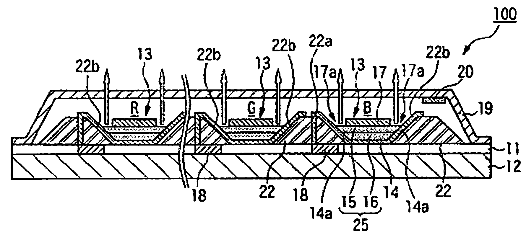
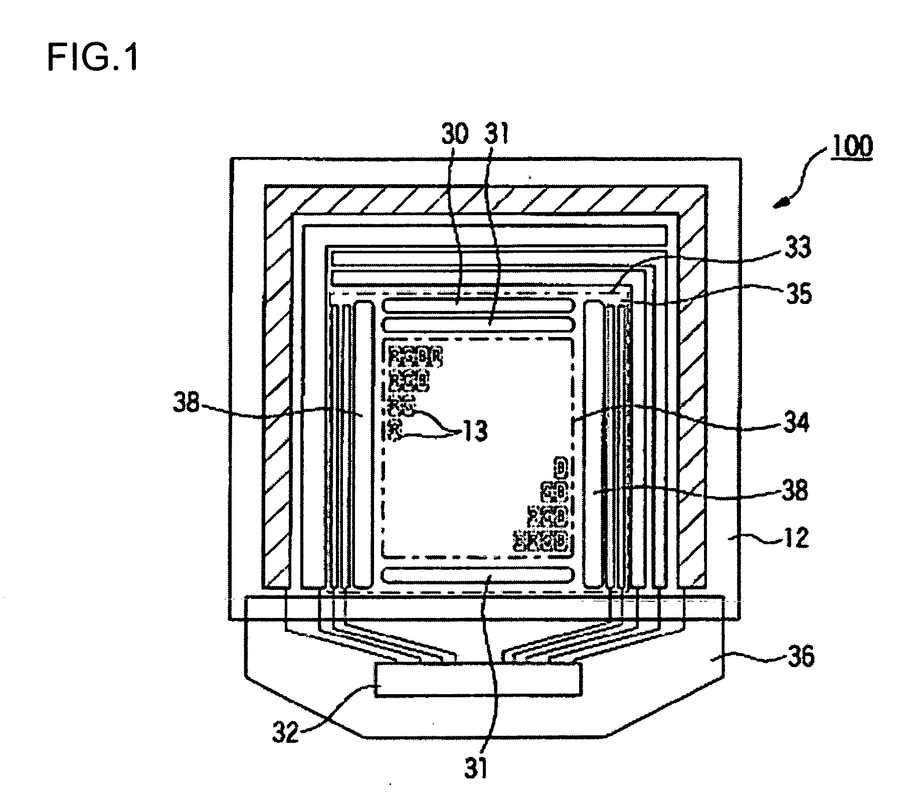
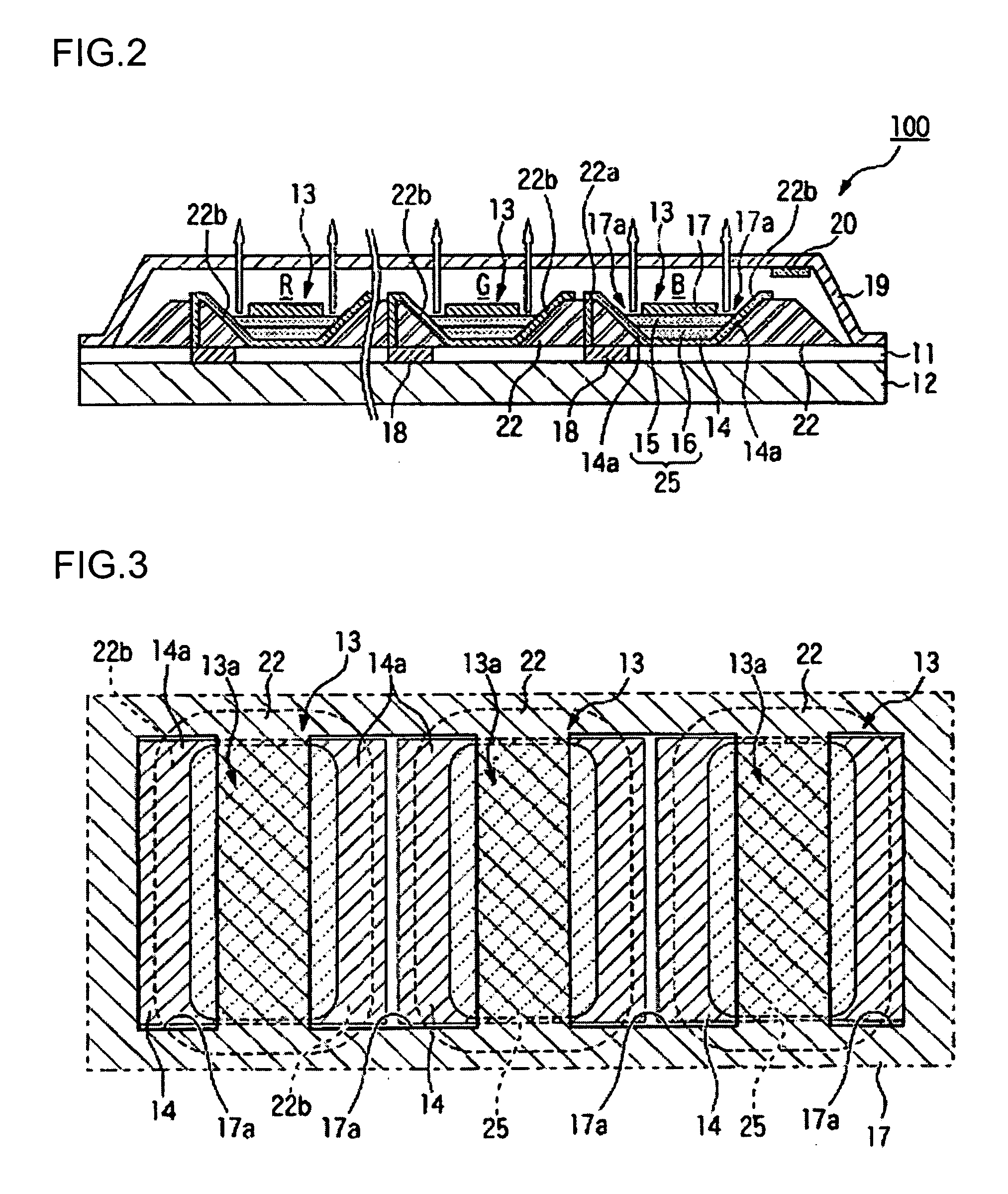
[0089]FIG. 1 is an overall plan view of the construction of an organic electroluminescent (organic EL) device according to an embodiment of a light-emitting device of the present invention, FIG. 2 is a partial cross-sectional view of the organic EL device, and FIG. 3 is a plan view of the construction of a plurality of light-e...

second embodiment

[0115] Next, a second embodiment of the present invention will be described with reference to FIG. 4. FIG. 4 is a partial cross-sectional view showing the construction of an organic EL device 110 of the present embodiment, and corresponds to FIG. 2 in the organic EL device 100 of the first embodiment. In FIG. 4, the sealing substrate is not shown, but the organic EL device 110 of the present embodiment has the same elements as those of the organic EL device 100 described above, except that inside the bank 22 dividing the respective light-emitting elements, a sub-bank (inner partition) 32 is provided to additionally divide the corresponding region. Therefore, in the following description and FIG. 4, the same elements as those of the first embodiment are represented by the same reference numerals, and the descriptions on the same elements will be omitted.

[0116] The organic EL device 110 shown in FIG. 4 comprises a plurality oflight-emitting elements 53. The respective light-emitting ...

third embodiment

[0119] Next, a third embodiment of the present invention will be described with reference to FIG. 5. FIG. 5 is a partial cross-sectional view showing the construction of an organic EL device 120 of the present embodiment and corresponds to FIG. 2 in the organic EL device 100 of the first embodiment.

[0120] Moreover, in FIG. 5, the sealing substrate is omitted. Further, in the present embodiment, different elements from those of the embodiments described above will be described. In addition, the same elements as those of the embodiments described above are represented by the same reference numerals, and the description thereon will be omitted.

[0121] The organic EL device 120 of the present embodiment has the same basic construction as that of the embodiments described above, a bank (partition) 60, a cathode (second electrode) 62 and an interlayer insulating film 64.

[0122] Here, in the bank 60, a first bank layer 60a, a second bank layer 60b and a third bank layer 60c are sequential...


PUM


Abstract

The invention provides a light-emitting device, a manufacturing method thereof, and an electronic apparatus which can improve the emission efficiency of light, obtain uniform brightness within a display surface in high reliability, in particular, and which can suppress lowering of the emission efficiency of light due to various wiring line structures, even though a large screen is performed. In a light-emitting device having a light-emitting element in which a first electrode on a base substrate, a functional layer having a light-emitting layer, and a second electrode are sequentially deposited, the first electrode and the second electrode are reflective, and the second electrode has an opening through which light from the light-emitting layer passes.

Description

BACKGROUND OF THE INVENTION [0001] 1. Field of Invention [0002] The present invention relates to a light-emitting device, such as a liquid crystal device, an organic EL (electroluminescent) device or an inorganic EL device, a manufacturing method of the light-emitting device, and an electronic apparatus in which the light-emitting device is mounted. [0003] 2. Description of Related Art [0004] Conventionally, in light-emitting devices such as organic electroluminescent (hereinafter, referred to as organic EL) devices, a plurality of circuit elements, an anode, a hole injection layer, a light-emitting layer made of an electro-optical material such as an EL material, a cathode and so on are deposited on a substrate, and then a sealing substrate is provided, with these elements interposed between the substrates. More specifically, an anode made of a transparent conductive material such as indium tin oxide (ITO) or tin oxide (SnO2), a hole injecting layer made of a dopant such as polythi...

Claims


Application Information

Patent Timeline
IPC IPC(8): G09F9/30G09G3/36H05B33/24H01J1/62H01L27/32H01L31/06H01L51/50H01L51/52H05B33/00H05B33/10H05B33/12H05B33/14H05B33/22H05B33/26H05B33/28
CPCH01L27/3246H01L27/3276H01L51/5218H01L2251/5315H01L51/5234H01L51/5268H01L51/5271H01L51/5228H10K59/122H10K59/131H10K50/818H10K50/824H10K50/828H10K50/854H10K50/856H10K2102/3026H05B33/26H05B33/10
Inventor KOBAYASHI, HIDEKAZU
Owner SEIKO EPSON CORP
Why Eureka
Try Eureka