
Plasma display panel

a technology of display panel and plasma, which is applied in the direction of address electrodes, gas-filled discharge tubes, gas discharge vessels/containers, etc., can solve the problems of reducing the luminescent efficiency of 3-electrode surface discharge pdp b>1/b>, affecting the luminescent efficiency of the y electrode, and reducing the distance between the address electrode and the y electrode, so as to reduce the distance between the substrate and the address electrod

Inactive Publication Date: 2005-06-02
SAMSUNG SDI CO LTD
View PDF15 Cites 47 Cited by
  • Summary
  • Abstract
  • Description
  • Claims
  • Application Information

AI Technical Summary

Benefits of technology

[0014] It is also an object to provide a design for a plasma display panel that is capable of being driven with low voltage and at high speed by reducing a distance between an address electrode and a Y electrode without decreasing the distance between the substrates.
[0015] It is further an object of the present invention to provide a design for a PDP where a gap between the address electrodes and the discharge electrodes is reduced without incurring any degradation in image quality.

Problems solved by technology

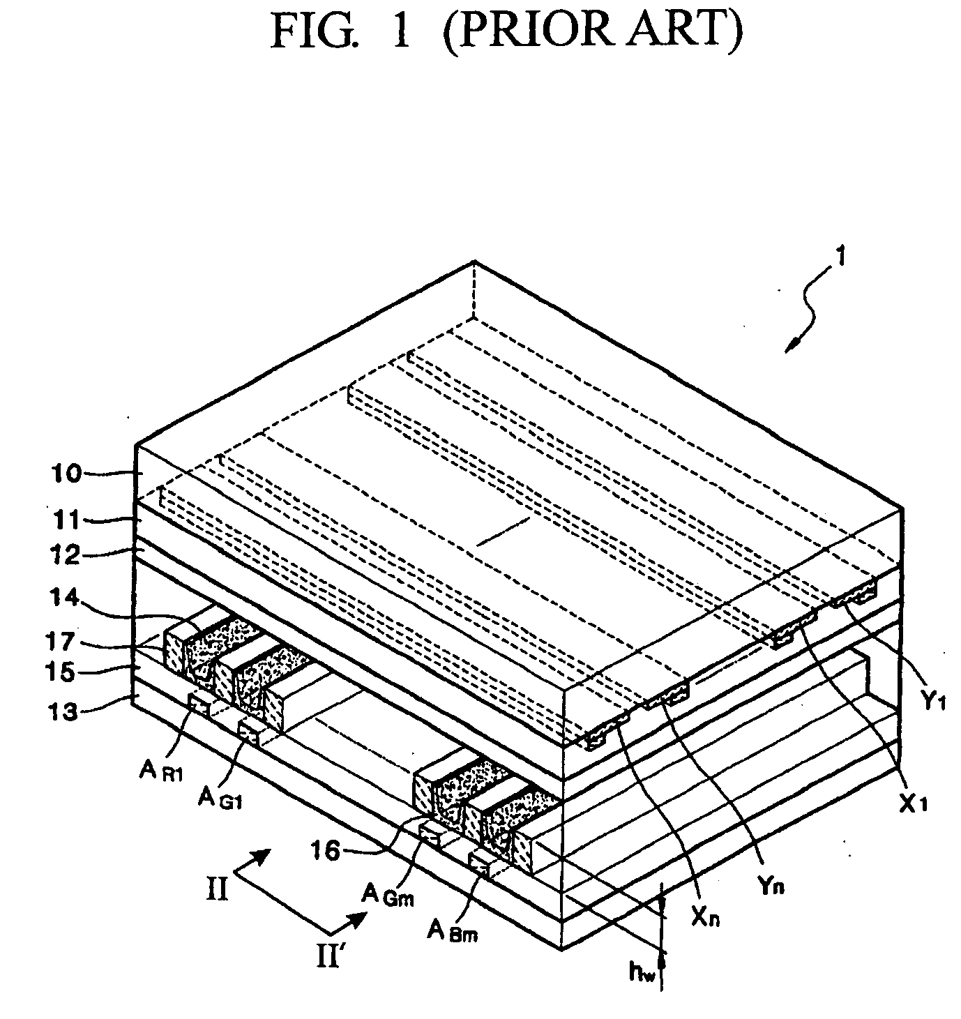
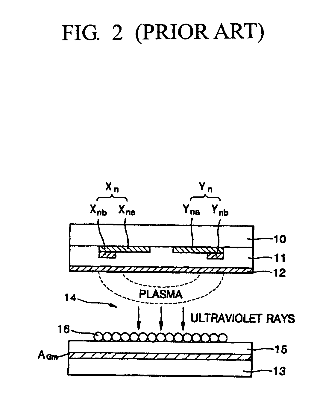
However, the 3-electrode surface discharge PDP 1 has a significant problem in that only about 60% of the visible rays are transmitted through the front substrate 10 because of various components formed on the front substrate 10.
Hence, the 3-electrode surface discharge PDP 1 has low luminescent efficiency.
These electrodes formed on the inner surface of the front substrate tend to block some of the visible rays generated, thus leading to losses.
In other words, a great distance between the address electrode and the Y electrode requires a very large voltage, which requires high power consumption.
Thus, attempts to lower power consumption by reducing barrier rib height can deteriorate the image quality.
If the barrier ribs are made shorter to lower the power consumption, brightness suffers.
If the barrier ribs are made high, the distance between the address and the Y electrodes increase leading to higher power consumption.

Method used


Image

  • Plasma display panel
  • Plasma display panel
  • Plasma display panel

Examples


Embodiment Construction

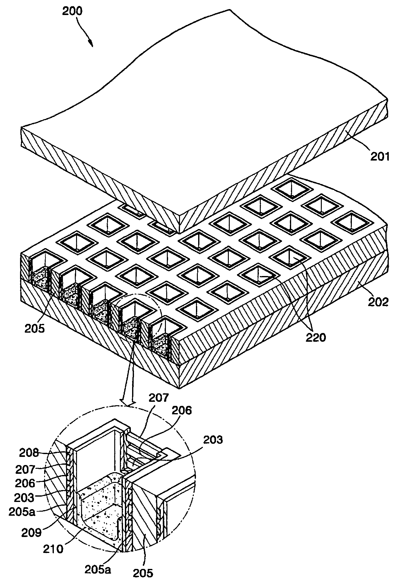
[0028] Turning now to FIGS. 3 through 8, these figures illustrate PDPs 200, 300 and 400 according to embodiments of the present invention. Referring to FIG. 3, a plasma display panel 200 according to an embodiment of the present invention includes a front substrate 201 facing a rear substrate 202 and spaced apart from each other by a predetermined distance. Barrier ribs 205 divide a space between the substrates into a plurality of discharge spaces 220. The barrier ribs 205 may be arranged in various patterns as long as the discharge spaces 220 can be formed. For example, the barrier ribs 205 may be not only open barrier ribs, such as strips, but also closed barrier ribs, such as ribs forming a waffle, a matrix, a delta shape, or the like. In FIGS. 3 through 8, the barrier ribs are illustrated as being closed barrier ribs, and the closed barrier ribs 205 are formed such that each of the discharge spaces 220 has a rectangular horizontal cross-section. However, the horizontal cross-sec...


PUM


Abstract

A plasma display panel capable of being fast driven with low voltage by reducing a distance between an address electrode and a Y electrode. The plasma display panel includes a pair of substrates, discharge electrodes, and an address electrode. The substrates are arranged at a predetermined interval to face each other and form a plurality of discharge spaces between facing surfaces of the substrates. The discharge electrodes are arranged at predetermined intervals between the substrates. The address electrode is arranged a predetermined distance apart from the discharge electrodes in a direction where the substrates are arranged, and defines each of the discharge spaces in cooperation with the discharge electrodes.

Description

[0001] This application makes reference to, incorporates the same herein, and claims all benefits accruing under 35 U.S.C. §119 from an application for PLASMA DISPLAY PANEL earlier filed in the Korean Intellectual Property Office on 29 Nov. 2003 and thereby duly assigned Serial No. 2003-86069. BACKGROUND OF THE INVENTION [0002] 1. Field of the Invention [0003] The present invention relates to a plasma display panel, and more particularly, to a design for a plasma display panel that is capable of being driven using only low voltages at a high speed by reducing a distance between an address electrode and a Y electrode. [0004] 2. Description of the Related Art [0005] A plasma display panel (PDP) display, which is a recent flat panel display, has excellent characteristics, such as the display of a quality image, being extremely thin and light, providing a wide viewing angle while having a large screen. In addition, a PDP display can be more simply manufactured than other flat panel disp...

Claims


Application Information

Patent Timeline
IPC IPC(8): H01J11/14H01J11/16H01J11/22H01J11/24H01J11/26H01J11/32H01J11/34H01J11/36
CPCH01J11/16H01J2211/363H01J11/36H01J11/24H01J11/38
Inventor YOO, HUN-SUKYI, WON-JUKANG, KYOUNG-DOO
Owner SAMSUNG SDI CO LTD
Learn More