Photosensitive display panel

a technology of liquid crystal display panel and light sensor, which is applied in the direction of static indicating device, radio frequency controlled device, instrument, etc., can solve the problems of increasing the cost and size of the apparatus, adversely affecting optical performance, and needing extra components, etc., to achieve simplified circuitry, less circuitry, and more cost efficient and bright

Active Publication Date: 2005-06-02
SAMSUNG DISPLAY CO LTD
View PDF2 Cites 70 Cited by
  • Summary
  • Abstract
  • Description
  • Claims
  • Application Information

AI Technical Summary

Benefits of technology

[0016] The present invention is directed to a light sensing display panel, a light-sensitive device including the light sensing display panel, and a method of driving the light sensing display panel. The invention allows a light-sensitive (i.e., a touch-sensitive) display device to be made with less circuitry than in the currently available light-sensitive display devices. With simplified circuitry, the display device of the invention is more cost efficient and brighter than the currently available devices.

Problems solved by technology

The need for extra components is disadvantageous, as it adds to the cost and size of the apparatus.
Further, in some cases, the extra component (e.g., a touch panel) reduces the display transmittance, adversely affecting optical performance.
However, when a transmissive LCD apparatus or a transflective LCD apparatus includes the light sensing element, the presence of the extra circuitry results in a decreased pixel aperture.
One of the disadvantages of the integrated touch screen display panel shown in FIG. 1 is that the light sensing element contains two switching elements (e.g., thin film transistors) and one capacitor.
This complicated structure of the light sensing element results in a complex array substrate circuitry, which makes the array substrate production difficult and decreases the yield.
Furthermore, the highly complex circuitry makes it more likely that signal interference will form between elements in the pixel region.
An integrated optical touch screen that does not increase the cost or size of the display panel and does not decrease the performance of the display panel is desired.

Method used


Image

  • Photosensitive display panel
  • Photosensitive display panel
  • Photosensitive display panel

Examples


Embodiment Construction

[0030] Embodiments of the invention are described herein in the context of a liquid crystal display (LCD) apparatus. However, it is to be understood that the embodiments provided herein are just preferred embodiments, and the scope of the invention is not limited to the applications or the embodiments disclosed herein.

[0031] As used herein, “light” or “incident light” refers to radiation from a source outside of the display apparatus that is incident on a photosensitive switch and having an intensity above or below a preselected threshold level. A “photosensitive switch” applies a signal to a read-out line in response to incident light. Two components that are “directly electrically connected” do not have intervening components between the two components. In contrast, two components that are “electrically connected” or “electrically coupled” may be directly connected (i.e., without intervening components) or connected through one or more intervening components.

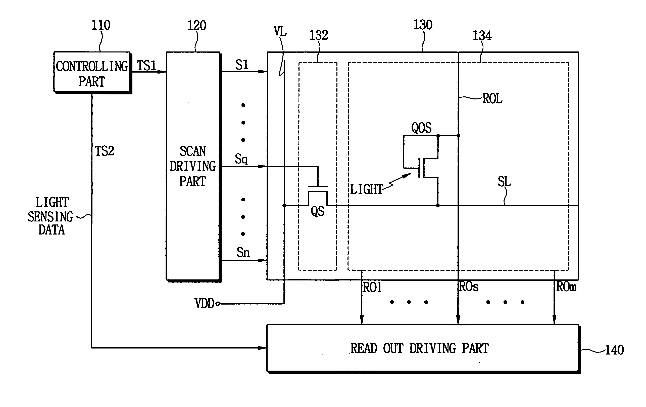
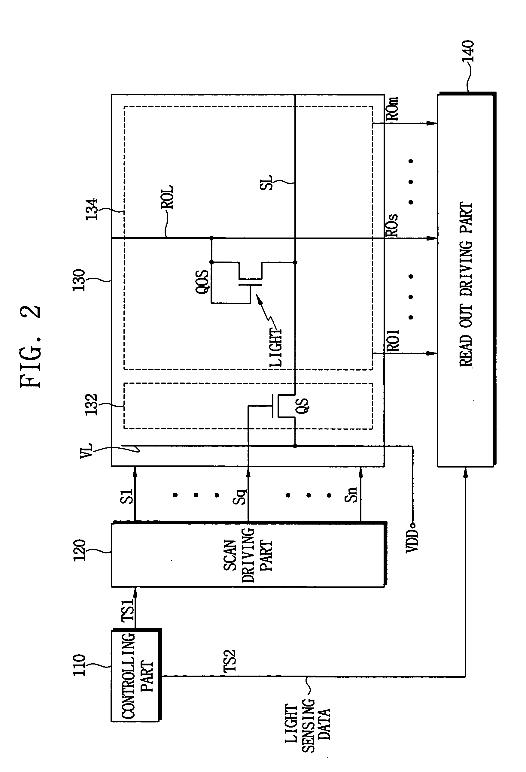
[0032]FIG. 2 is a pl...


PUM

PropertyMeasurementUnit
bias voltageaaaaaaaaaa
gate-source voltageaaaaaaaaaa
bias voltageaaaaaaaaaa

Abstract

A light-sensitive (i.e., touch-sensitive) display device that requires less circuitry than the currently available light-sensitive display devices is presented. Unlike the currently available devices, which require at least two switching elements and a capacitor to implement a photosensitive switch, the invention only requires one switching element. The device of the invention includes a substrate with a plurality of scan lines, a plurality of read-out lines, a power line, and an array of photosensitive switches formed thereon. The scan lines and the read-out lines extend in directions that are substantially perpendicular to each other, forming pixels. One photosensitive switch is formed in each pixel, and each photosensitive switch has one light-sensitive transistor. The transistor connects the power line to one of the read-out lines in response to sensing incident light.

Description

RELATED APPLICATION(S) [0001] This patent application claims priority, under 35 U.S.C. § 119, from Korean Patent Application No. 2003-86184 filed on Dec. 1, 2003, the content of which is incorporated by reference herein in its entirety.BACKGROUND OF THE INVENTION [0002] 1. Field of the Invention [0003] The invention relates generally to a light sensing panel and particularly to a light sensing liquid crystal display panel. [0004] 2. Discussion of the Related Art [0005] Touch screens have become popular in various display applications such as PDAs and other computer products. Some touch screens are used with active matrix liquid crystal display (LCD) apparatuses. Most of the touch-enabled LCD apparatuses are based on resistive, capacitive, or inductive touch technology, which requires extra components that are typically not integrated into the LCD apparatuses, such as a touch panel. The need for extra components is disadvantageous, as it adds to the cost and size of the apparatus. Fu...

Claims


Application Information

Patent Timeline
Patent Type & Authority Applications(United States)
IPC IPC(8): G02F1/1345G02F1/133G02F1/1368G06F3/03G06F3/033G06F3/041G06F3/042G06T1/00G09G3/36G09G5/00H01L21/00H01L27/146
CPCG06F3/042G06F3/0412G09G3/36
Inventor CHOI, JOON-HOOJOO, IN-SUKIM, HYUNG-GUEL
Owner SAMSUNG DISPLAY CO LTD
Why Eureka
Try Eureka