Optical waveguide module

a technology of optical waveguides and modules, applied in the direction of optical waveguide light guides, instruments, optics, etc., can solve the problems of increasing the number of optical components, increasing the complexity of varying the photosensitivity of the reflected light at the photodetector, so as to simplify the structure and manufacturing process of the optical circuit.

Inactive Publication Date: 2005-06-02
SUMITOMO ELECTRIC IND LTD
View PDF7 Cites 25 Cited by
  • Summary
  • Abstract
  • Description
  • Claims
  • Application Information

AI Technical Summary

Benefits of technology

[0004] A problem with this use of an optical coupler, though, is that it increases the number of optical components that make up the optical circuit and furthermore, since these have to be fused together, the structure and the manufacturing process of the optical circuit become more complicated.
[0007] The present invention has been accomplished in order to solve the above problem, and it is an object thereof to provide an optical waveguide module, with which the optical intensity can be correctly monitored regardless of the state of polarization of the signal light.
[0009] With the above-mentioned optical waveguide module, rather than the optical waveguide being split with an optical coupler, part of the signal light is reflected by a reflection filter, which is disposed in an inclined groove provided to the optical waveguide, and the optical intensity of the signal light can be monitored by means of the reflected light. As a result, the structure and manufacturing process of the optical circuit are simplified.
[0010] Also, there is adopted a constitution made such that the reflected light from the reflection filter is made incident onto the light incident face of the photodetector at a predetermined angle with respect thereto. Here, since the polarization dependence of the light, which passes through the light incident face, is reduced, the photosensitivity for the reflected light at the photodetector can be kept approximately constant regardless of the state of polarization of the signal light. As a consequence, it is made possible to monitor the optical intensity correctly regardless of the state of polarization of the signal light.

Problems solved by technology

A problem with this use of an optical coupler, though, is that it increases the number of optical components that make up the optical circuit and furthermore, since these have to be fused together, the structure and the manufacturing process of the optical circuit become more complicated.
Here, there occurs a problem in that the photosensitivity for the reflected light at the photodetector varies with polarization states of the signal light, due to the polarization dependence of the light, which passes through the light incident face.

Method used


Image

  • Optical waveguide module
  • Optical waveguide module
  • Optical waveguide module

Examples


first embodiment

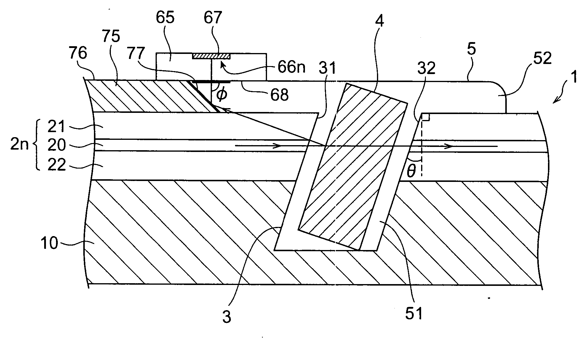
[0032]FIG. 1 is a plan view of a structure of an optical waveguide module in accordance with the present invention. The optical waveguide module comprises an optical circuit 1 which are constituted of a substrate 10, and 8 optical waveguides 21-28 (8 channels) disposed on the substrate 10. In this embodiment, for the optical waveguides 21-28, an optical waveguide of planar optical waveguide type, which are formed on the substrate 10, are employed.

[0033] Each of the optical waveguides 21-28 is formed parallel to each other at regular intervals along a predetermined optical transmission direction (the direction indicated by the arrowheads in FIG. 1) from input end 11 toward output end 12 of a planar optical waveguide type optical circuit 1. Also, at a predetermined portion with respect to the optical transmission direction of the planar optical waveguide type optical circuit 1, a groove 3, which crosses the optical waveguides 21-28, is formed.

[0034] Inside the groove 3, a reflection ...

fourth embodiment

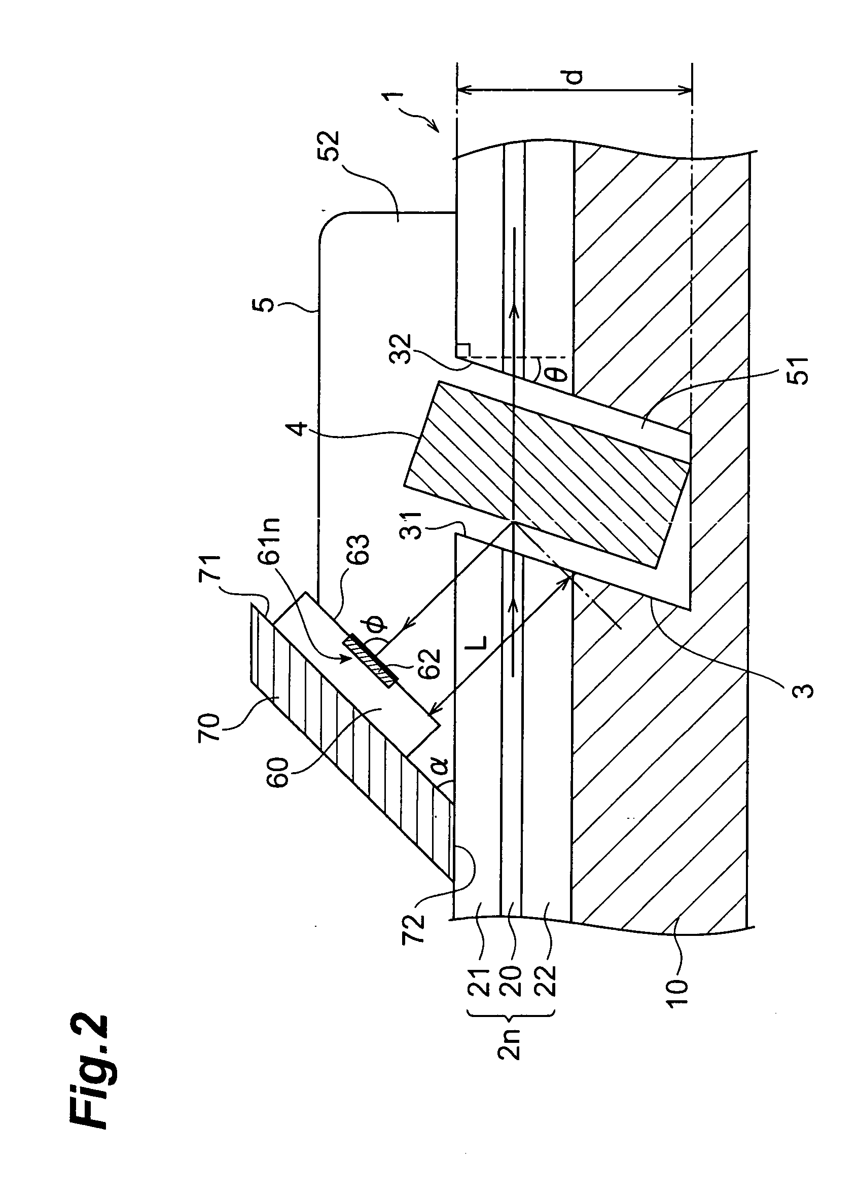
[0121]FIG. 13 is a cross sectional view showing a structure of cross section of the optical waveguide module along the direction of the optical axis of an optical waveguides 2n (n=1−8). In FIG. 13, a portion including a groove 3, a reflection filter 4 and photodetector array 85 is shown enlarged. Also, in the constitution shown in FIG. 13, the planar optical waveguide type optical circuit 1 including optical waveguides 2n comprised of the lower clad 22, the core 20 and the upper clad 21, the groove 3, the reflection filter 4 and the filler resin 5 are the same as those in the constitution in FIG. 2.

[0122] The optical waveguide module according to this embodiment has almost the same constitution as that of the first embodiment shown in FIG. 1 and FIG. 2. Hence, in this embodiment, the plan view is omitted. To be more specific, the optical waveguide module according to this embodiment is different from the first embodiment in the constitution of the sub-mounting substrate or the like...


PUM


Abstract

In a planar optical waveguide type optical circuit 1, a reflection filter 4 is installed on the inside of a inclined groove 3, which is formed so as to cross optical waveguides 2n. Reflected light from the reflection filter 4 is detected by photodetectors 61n of a photodetector array 60, thereby the optical intensity of the signal light is monitored. As for the photodetectors 61n, there is adopted a constitution such that a sub-mounting substrate 70 is disposed at the top side of the optical circuit 1 to hold the photodetector array 60 with a photodetector mounting face 71, which is inclined at an angle α (0°<α<90°) with respect to the top surface of the optical circuit 1 such that the reflected light from the reflection filter 4 is made incident onto a light incident face 63 of the photodetectors 61n in the photodetector array 60 at a predetermined angle φ. As a consequence, an optical waveguide module, which is capable of monitoring the optical intensity correctly regardless of the polarization state of the signal light, is obtained.

Description

TECHNICAL FIELD [0001] The present invention relates to an optical waveguide module having an optical waveguide formed on a substrate. BACKGROUND ART [0002] In an optical circuit, which makes use of an optical waveguide such as an optical fiber or planar optical waveguide, it is sometimes desirable to control the optical intensity of signal light to a suitable value, such as keeping the optical intensity constant for signal light transmitted through optical waveguides. In such a case, the optical intensity of the signal light is monitored in the optical circuit, and sometimes the optical intensity is also controlled on the basis of the results of this monitoring. DISCLOSURE OF THE INVENTION [0003] This monitoring of the optical intensity of signal light used to be accomplished by providing an optical coupler on an optical waveguide and splitting part of the signal light. With this method, an optical coupler is provided at a specific location along the optical waveguide, a few percen...

Claims


Application Information

Patent Timeline
Patent Type & Authority Applications(United States)
IPC IPC(8): G02B6/12G02B6/36G02B6/42
CPCG02B6/3636G02B6/3652G02B6/42G02B6/4212G02B2006/12109G02B6/4246G02B6/4249G02B2006/12104G02B6/4214G02B6/43
Inventor KOMIYA, TAKEOSASAKI, TAKASHIFUJIMURA, YASUSHIKATSUYAMA, TSUKURUYAMABAYASHI, NAOYUKI
Owner SUMITOMO ELECTRIC IND LTD
Why Eureka
Try Eureka