Method of the adjustable matching map system in lithography

a mapping system and map technology, applied in the field of integrated circuit fabrication, can solve the problems of optical projection system error, mask to mask error, and the location of reference marks outside the device pattern does not provide the accuracy of overlaying a second layer pattern to a first layer pattern. the effect of improving the accuracy of overlaying a second layer pattern

Inactive Publication Date: 2005-06-02
TAIWAN SEMICON MFG CO LTD
View PDF5 Cites 34 Cited by
  • Summary
  • Abstract
  • Description
  • Claims
  • Application Information

AI Technical Summary

Benefits of technology

[0011] One objective of the present invention is to provide a method of determining mask to mask error that improves the accuracy of overlaying a second layer pattern on a first pattern on a semiconductor substrate.
[0013] A still further objective of the present invention is to provide a method that reduces layer to layer overlay error for printing a second layer pattern on a first layer pattern on a substrate.
[0017] The measurement results for each grid square are inputted into a correction algorithm that adjusts exposure tool settings such as field rotation, magnification, x and y stage scale, orthogonality, and offset translation for each exposure field in subsequent exposures with the second mask. The exposure tool adjustments will enable a more accurate overlay of the second photoresist pattern on the first pattern when processing subsequent substrates.

Problems solved by technology

There are two major factors contributing to this overlay error which is also called layer to layer error.
One is optical projection system error and the other is mask to mask error.
For advanced technologies that are approaching nodes of 100 nm or less, the location of reference marks outside the device pattern does not provide a second layer pattern to first layer pattern overlay accuracy that satisfies current overlay specifications.

Method used


Image

  • Method of the adjustable matching map system in lithography
  • Method of the adjustable matching map system in lithography
  • Method of the adjustable matching map system in lithography

Examples


first embodiment

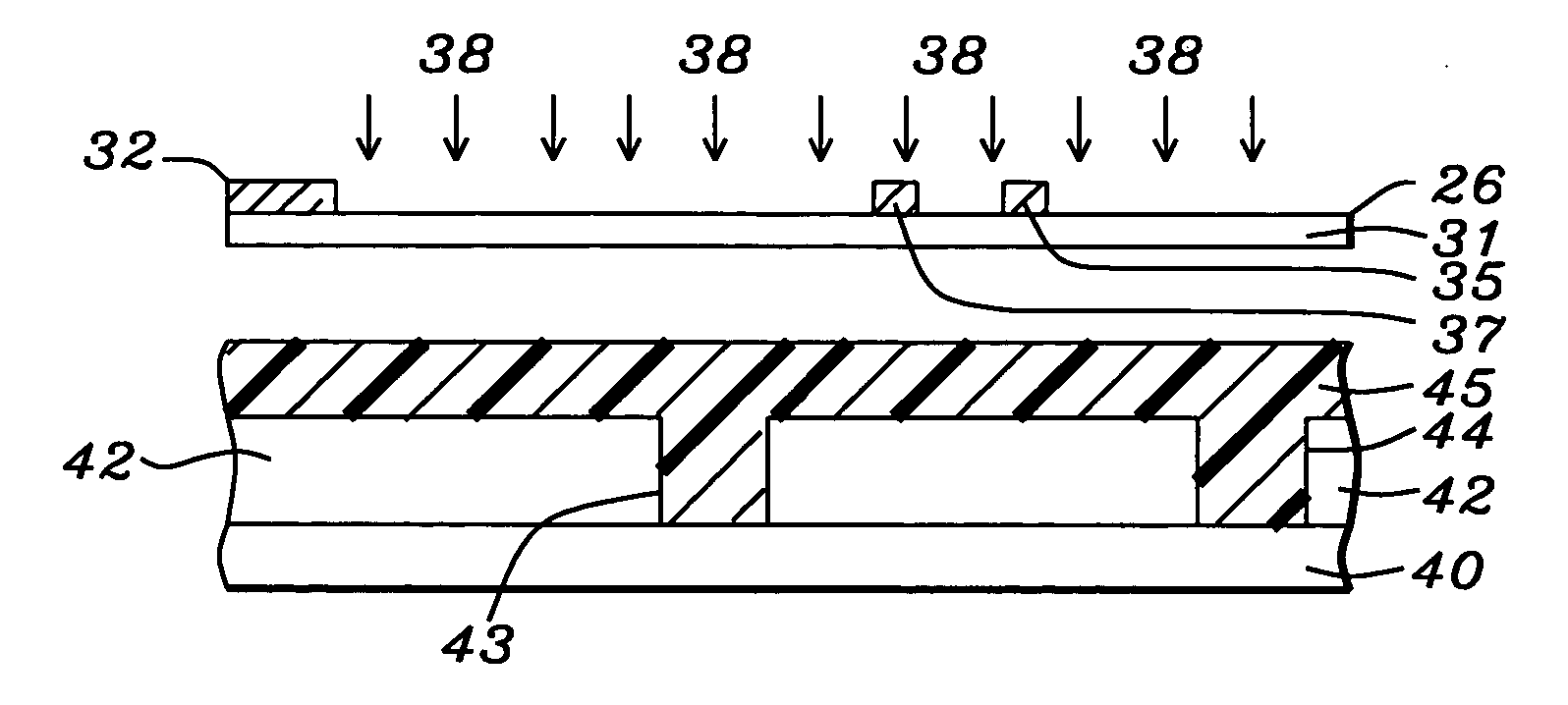
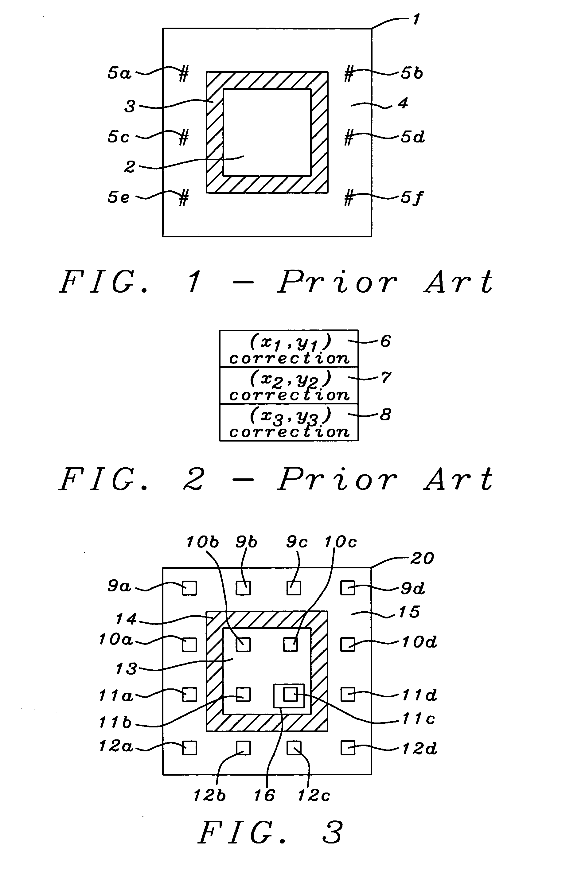
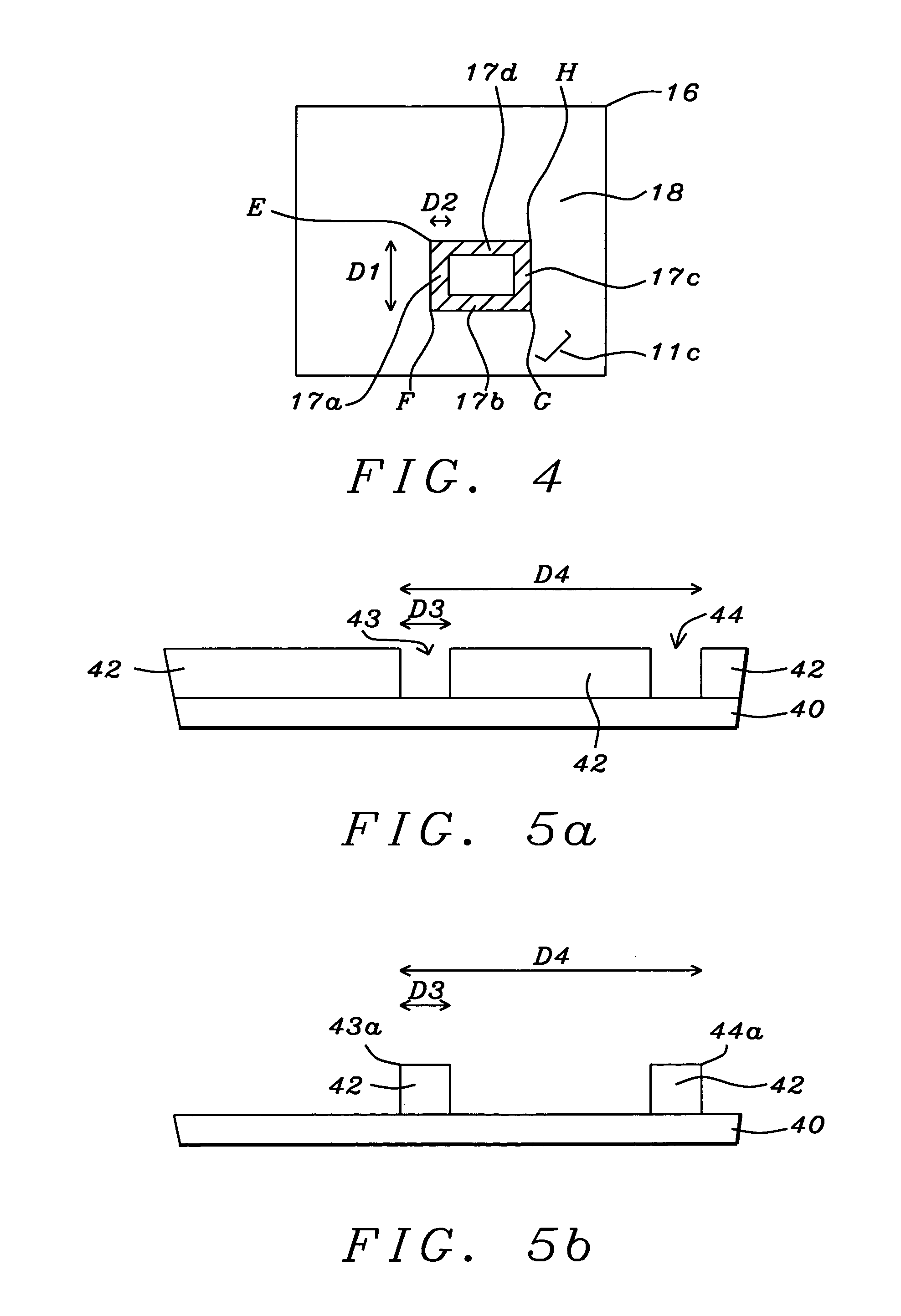
[0037] In the first embodiment, a method is provided for determining the overlay error of a second layer pattern on a first layer pattern in a substrate. The error measurements are used to make corrections in exposure tool settings that will generate a more accurate placement of the second layer pattern on the first layer pattern in subsequent substrates. Referring to FIG. 3, a first layer mask 20 is shown that is comprised of an inner first layer pattern area 13, a chrome forbidden area 14, and an outer region 15. The outer region 15 may be opaque or transparent depending on the type of mask. A key feature of the invention is that first reference marks 10b, 10c, 11b, 11c are inserted within the first layer pattern area 13 in order to provide a more accurate determination of layer to layer overlay in a subsequent step. Conventional masks only have reference marks in a region 15 outside the forbidden area 14.

second embodiment

[0038] Note that other first reference marks 9a-9d, 10a, 10d, 11a, 11d, and 12a-12d may be placed in the outer region 15 and their use will become apparent during a description of mask to mask overlay in a Although a 2×2 array of first reference marks is shown within the first layer pattern area 13, optionally, an “m” x “n” array may be used. Alternatively, a different sized array of first reference marks may be used instead of the 4×4 array that covers the first layer mask 20.

[0039] In one embodiment, the first reference marks are comprised of chrome that is placed on a transparent region of a first layer mask 20. The first reference marks are placed at least 2 microns from any pattern features in the first layer pattern area 13. In an alternative embodiment in which the first layer mask is an attenuated or alternating phase shifting mask, the first reference marks are constructed so that light passing through the marks is transmitted 180° out of phase with light that passes throu...


PUM

PropertyMeasurementUnit
lengthaaaaaaaaaa
widthaaaaaaaaaa
lengthaaaaaaaaaa

Abstract

A method is provided for improving layer to layer overlay of a second layer pattern on a first layer pattern formed in a substrate. A plurality of first reference marks is placed inside a pattern area on a first layer mask which is used to form the first layer pattern. A plurality of second reference marks is placed on a second layer mask which is used to form the second layer pattern and in which one second reference mark is matched with a first reference mark having the same (x,y) coordinates. Reference mark placement in the resulting first and second layer patterns is determined by metrology to determine an x-deviation and a y-deviation for each matched pair of reference marks. A correction algorithm is then used to calculate adjustments in exposure tool settings for improved overlay of the second layer pattern on the first layer pattern in subsequent exposures.

Description

FIELD OF THE INVENTION [0001] The invention relates to a method of fabricating an integrated circuit in a semiconductor device. More particularly, the present invention relates to a method of more accurately aligning a second layer pattern formed in a photoresist layer on a first layer pattern formed in a substrate. BACKGROUND OF THE INVENTION [0002] Photoresist patterning is a key step in the formation of integrated circuits in semiconductor devices. A photoresist layer is typically spin coated on a substrate and patternwise exposed by employing an exposure tool and a mask that contains a device pattern. The mask may be comprised of an opaque material such as chrome on a transparent substrate like quartz. Other masks called phase shifting masks have regions that transmit light which is 180° out of phase with light transmitted through an adjacent region. Radiation is transmitted through a mask to selectively expose portions of the photoresist layer which are later developed in a med...

Claims


Application Information

Patent Timeline
Patent Type & Authority Applications(United States)
IPC IPC(8): G03F7/00G03F7/20G03F9/00
CPCG03F7/70633G03F7/0035
Inventor TSAI, FEI-GWO
Owner TAIWAN SEMICON MFG CO LTD
Why Eureka
Try Eureka