Simulation model for designing semiconductor devices, apparatus for simulating the designing of semiconductor devices, method of simulating the designing of semiconductor devices, computer-readable recording medium storing a program for simulating the designing of semiconductor devices, semiconductor device, and method of manufacturing the semiconductor device

a simulation model and semiconductor technology, applied in the direction of individual semiconductor device testing, semiconductor/solid-state device testing/measurement, instruments, etc., can solve the problems of difficult to predict or reproduce the behavior of the carrier, difficult to converge the device, and not practicably obtained in most models, so as to improve the analysis precision of the behavior, predict or reproduce the operation of the semiconductor element quickly, and improve the effect of the simulation model

Inactive Publication Date: 2005-06-02
SEMICON TECH ACADEMIC RES CENT
View PDF10 Cites 14 Cited by
  • Summary
  • Abstract
  • Description
  • Claims
  • Application Information

AI Technical Summary

Benefits of technology

[0011] The present invention has been developed in order to solve the above-described problems, and an object is to provide a simulation model for designing a semiconductor device, capable of predicting or reproducing an operation of a semiconductor element quickly within a practically allowable time regardless of a high / low operation speed with a high precision by enhancement of analysis precision of a behavior of a carrier in at least one place in one electrode to the other electrode not only in a stationary state but also in a transient state with respect to at least one semiconductor element having at least two electrodes.

Problems solved by technology

However, a satisfactory result is not practically obtained in most of the models.
Further in the third non-quasi-static model, it is difficult to converge the device.
The above-described problem could be caused generally in the semiconductor element having at least two electrodes concerned with transmission / reception of the carrier, for example, in a bipolar transistor or the like.
As described above, in the conventional non-quasi-static simulation model, it has heretofore been difficult to predict or reproduce the behavior of the carrier in the semiconductor device including the semiconductor element within a practically allowable time and with a high precision regardless of a stationary or transient state.
It is substantially impossible to especially predict or reproduce the behavior of the carrier in the semiconductor element or the semiconductor device which operates at a high speed using the simulation model with the high precision.
Moreover, needless to say, it is clearly difficult to simulate the operations of the semiconductor element and the semiconductor device within the practically allowable time and with high precision by a simulation apparatus, simulation method, or simulation program using the above-described simulation model.
Additionally, there is a possibility that performances of the semiconductor element and the semiconductor device designed or manufactured using the simulation model, simulation apparatus, simulation method, and simulation program are largely inferior to desired performances.

Method used


Image

  • Simulation model for designing semiconductor devices, apparatus for simulating the designing of semiconductor devices, method of simulating the designing of semiconductor devices, computer-readable recording medium storing a program for simulating the designing of semiconductor devices, semiconductor device, and method of manufacturing the semiconductor device
  • Simulation model for designing semiconductor devices, apparatus for simulating the designing of semiconductor devices, method of simulating the designing of semiconductor devices, computer-readable recording medium storing a program for simulating the designing of semiconductor devices, semiconductor device, and method of manufacturing the semiconductor device
  • Simulation model for designing semiconductor devices, apparatus for simulating the designing of semiconductor devices, method of simulating the designing of semiconductor devices, computer-readable recording medium storing a program for simulating the designing of semiconductor devices, semiconductor device, and method of manufacturing the semiconductor device

Examples


first embodiment

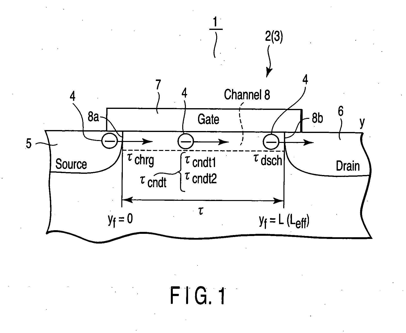
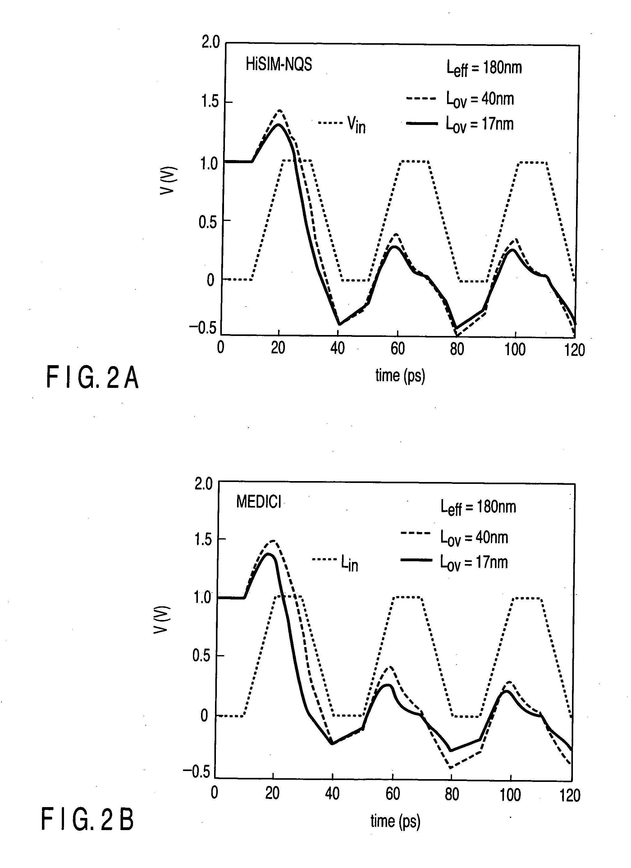
[0208] First, a first embodiment according to the present invention will be described with reference to FIGS. 1 to 6. FIG. 1 is a diagram schematically showing origin of an NQS effect of a simulation model for designing a semiconductor device according to the present embodiment. FIGS. 2A and 2B are graphs showing simulation results of voltage applications in the simulation model and a two-dimensional device simulation apparatus according to the present embodiment. FIG. 3 is a graph showing simulation results of displacement currents in the simulation model and the two-dimensional device simulation apparatus according to the present embodiment. FIG. 4 is a graph showing simulation results of transient drain currents in the simulation model and the two-dimensional device simulation apparatus according to the present embodiment. FIG. 5 is a graph showing a function of each delay model in transient carrier transport in the simulation model according to the present embodiment. FIG. 6 is ...

second embodiment

[0236] Next, a second embodiment according to the present invention will be described with reference to FIGS. 7 to 22.

[0237]FIG. 7 is a graph showing velocities of carriers in lateral directions in the transient state and quasi-static approximation at a high-speed switch-on time. FIG. 8 is a graph showing carrier concentrations in the transient state and quasi-static approximation on the side of the source of the MOSFET having a design rule of 0.5 μm. FIGS. 9A, 9B, 9C, and 9D are graphs showing charging delays of the carriers at a plurality of different rising times, and carrier velocity distributions in the transient state and quasi-static approximation at the plurality of different rising times. FIG. 10 is a graph showing a case where effects of the carrier charging delays are included and a case where the effects are not included in a simulation model according to the present embodiment. FIG. 11 is a diagram schematically showing analysis in a quasi-static state of a delay mecha...

third embodiment

[0275] Next, a third embodiment according to the present invention will be described with reference to FIGS. 23 to 30. FIG. 23 is a graph showing a relation between each of passing delay, charging delay, and two types of conductive delays which are delay models according to the present embodiment, and voltages. FIG. 24 is a graph showing calculation results of each carrier running time according to the present embodiment. FIG. 25 is a graph showing calculation results of each transient carrier density by the simulation model according to the present embodiment. FIG. 26 is a graph showing calculation results of conduction currents by the simulation model according to the present embodiment and two-dimensional device simulation. FIG. 27 is a graph showing calculation results of displacement currents by the simulation model according to the present embodiment and the two-dimensional device simulation. FIG. 28 is a graph showing dependence of the displacement current on the charging del...


PUM


Abstract

There is disclosed a simulation model for designing a semiconductor device, comprising adding at least a part of a difference between a density of a carrier described in a quasi-static manner with respect to a voltage applied between electrodes at a first time and a density of the carrier described in a transient state at a second time before the first time to the carrier density at the second time in accordance with a running delay of the carrier between both the times to thereby describe the carrier density at the first time in the transient state with respect to a semiconductor element having the first and second electrodes. A current flowing between the electrodes is described as a sum of a current flowing between the electrodes in the quasi-static manner, and a displacement current between the electrodes.

Description

CROSS-REFERENCE TO RELATED APPLICATIONS [0001] This application is based upon and claims the benefit of priority from the prior Japanese Patent Application No. 2003-318947, filed on Sep. 10, 2003; the entire contents of which are incorporated herein by reference. BACKGROUND OF THE INVENTION [0002] 1. Field of the Invention [0003] The present invention relates to a technique for designing a semiconductor device comprising at least one semiconductor element having at least two electrodes, particularly to a simulation model for designing a semiconductor device in which reproducibility of a behavior in a transition state of a carrier in each electrode and between the electrodes during a high-speed operation of a semiconductor element, an apparatus for simulating the designing of a semiconductor device, a method of simulating the designing of a semiconductor device, a computer-readable recording medium in which a program for simulating the designing of a semiconductor device, a semicondu...

Claims


Application Information

Patent Timeline
Patent Type & Authority Applications(United States)
IPC IPC(8): G06F17/50H01L21/00H01L21/336H01L21/82H01L29/00H01L29/78
CPCG06F17/5036G06F30/367
Inventor MIURA, MITIKONAKAYAMA, NORIAKI
Owner SEMICON TECH ACADEMIC RES CENT
Why Eureka
Try Eureka