Semiconductor nano-rod devices

a technology of semiconductors and nanorods, applied in the direction of transistors, solid-state devices, nanoinformatics, etc., can solve the problems of parasitic off-state leakage, gate oxide thickness, gate oxide thickness, etc., and achieve the effect of reducing the number of transistors

Inactive Publication Date: 2005-06-09
CHEN HAO YU +3
View PDF64 Cites 99 Cited by
  • Summary
  • Abstract
  • Description
  • Claims
  • Application Information

AI Technical Summary

Problems solved by technology

Hence, a transistor with a short gate length often suffers from problems related to the inability of the gate to substantially control the on / off states of the channel, which is often called short-channel effects.
However, for device scaling well into the sub-30 nm regime, the requirements for body-doping concentration, gate oxide thickness, and source / drain doping profiles become increasingly difficult to meet using conventional device structures based on bulk silicon substrates.
This may result in a parasitic off-state leakage.
However, this method requires a large amount of oxidation, and hence a large amount of oxide formation, to convert the rectangular channel cross-section shape to a rounded or circular channel cross-section.

Method used


Image

  • Semiconductor nano-rod devices
  • Semiconductor nano-rod devices
  • Semiconductor nano-rod devices

Examples


Embodiment Construction

[0017] The use of presently preferred embodiments are discussed in detail below. It should be appreciated, however, that the present invention provides many applicable inventive concepts that can be embodied in a wide variety of specific contexts. The specific embodiments discussed are merely illustrative of specific ways to make and use the invention, and do not limit the scope of the invention.

[0018] Example embodiments of the present invention will be described herein in a specific context of making semiconductor devices, such as transistors. In other embodiments not shown, embodiments of the present invention also may include nano-wires or quantum-wires formed in accordance with the present invention. The present invention may also be applied, however, to other situations.

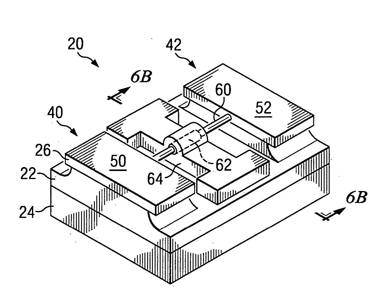
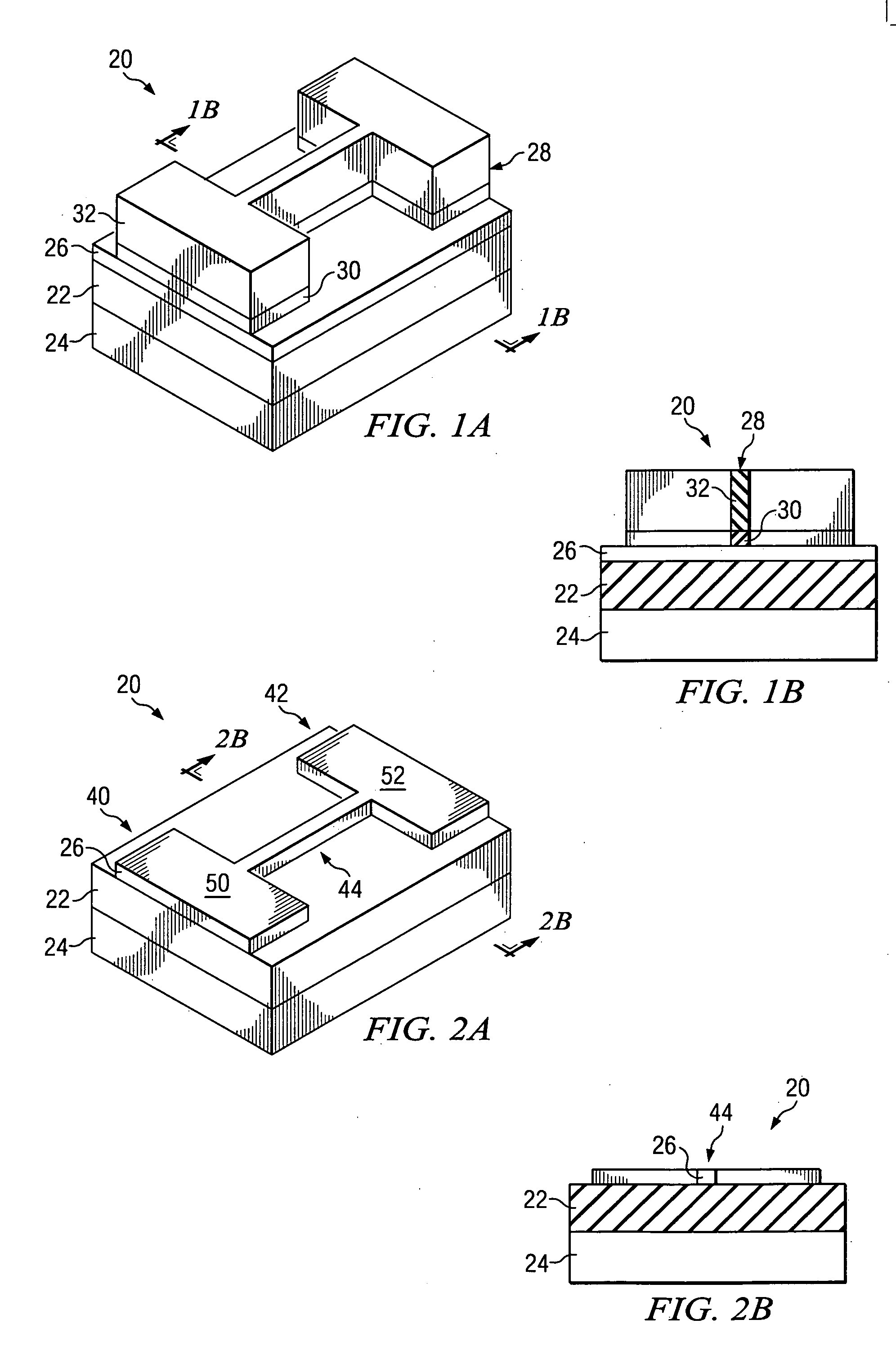
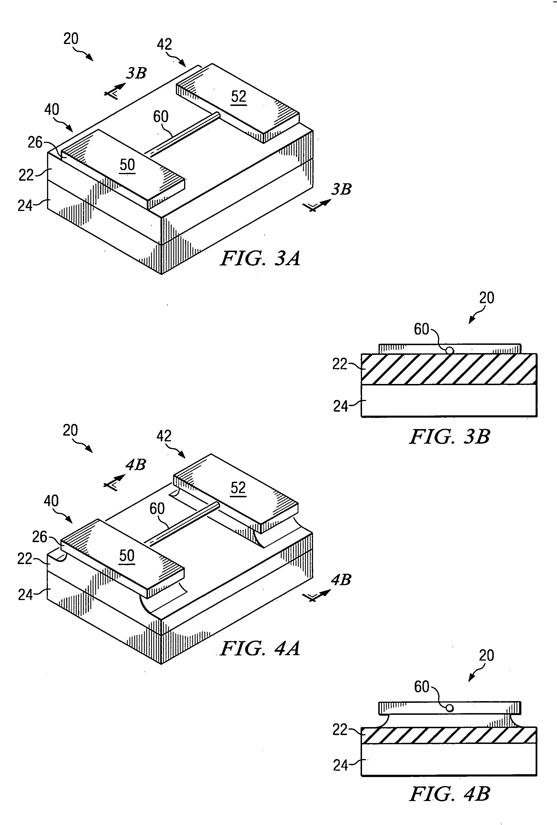
[0019] A preferred manufacturing process in accordance with the present invention may be used to make a transistor device. Some of the manufacturing steps of this preferred embodiment being used to make a tra...


PUM


Abstract

In a method of manufacturing a semiconductor device, a semiconductor layer is patterned to form a source region, a channel region, and a drain region in the semiconductor layer. The channel region extends between the source region and the drain region. Corners of the channel region are rounded by annealing the channel region to form a nano-rod structure. Part of the nano-rod structure is then used as a gate channel. Preferably, a gate dielectric and a gate electrode both wrap around the nano-rod structure, with the gate dielectric being between the nano-rod structure and the gate electrode, to form a transistor device.

Description

[0001] This application is a divisional of patent application Ser. No. 10 / 370,792, entitled “Semiconductor Nano-Rod Devices,” filed on Feb. 20, 2003, which application is incorporated herein by reference.TECHNICAL FIELD [0002] The present invention relates generally to methods for manufacturing semiconductor devices. In one aspect, the present invention relates to a method of forming a nano-rod structure for a channel of a field effect transistor. BACKGROUND [0003] Metal-oxide-semiconductor field effect transistor (MOSFET) technology is currently the dominant semiconductor technology used for manufacturing ultra-large scale integrated (ULSI) circuits. As the gate length of the MOSFET is scaled down into the sub-30 nm regime for improved performance and density, the source and drain increasingly interact with the channel to sometimes gain influence on the channel potential. Hence, a transistor with a short gate length often suffers from problems related to the inability of the gate t...

Claims


Application Information

Patent Timeline
Patent Type & Authority Applications(United States)
IPC IPC(8): H01L21/336H01L29/423H01L29/775H01L29/786
CPCB82Y10/00H01L29/0673H01L29/42384H01L29/7854H01L29/66742H01L29/66795H01L29/775H01L29/42392
Inventor CHEN, HAO-YUYEO, YEE-CHIAYANG, FU-LIANGHU, CHENMING
Owner CHEN HAO YU
Why Eureka
Try Eureka