Semiconductor device and the method of testing the same

Active Publication Date: 2005-06-09
RENESAS ELECTRONICS CORP
View PDF6 Cites 24 Cited by
  • Summary
  • Abstract
  • Description
  • Claims
  • Application Information

AI Technical Summary

Benefits of technology

[0020] (2) The semiconductor test equipment having the number of channels less tha

Problems solved by technology

This causes an increase in production costs.
Therefore, there arises the pro

Method used


Image

  • Semiconductor device and the method of testing the same
  • Semiconductor device and the method of testing the same
  • Semiconductor device and the method of testing the same

Examples


first embodiment

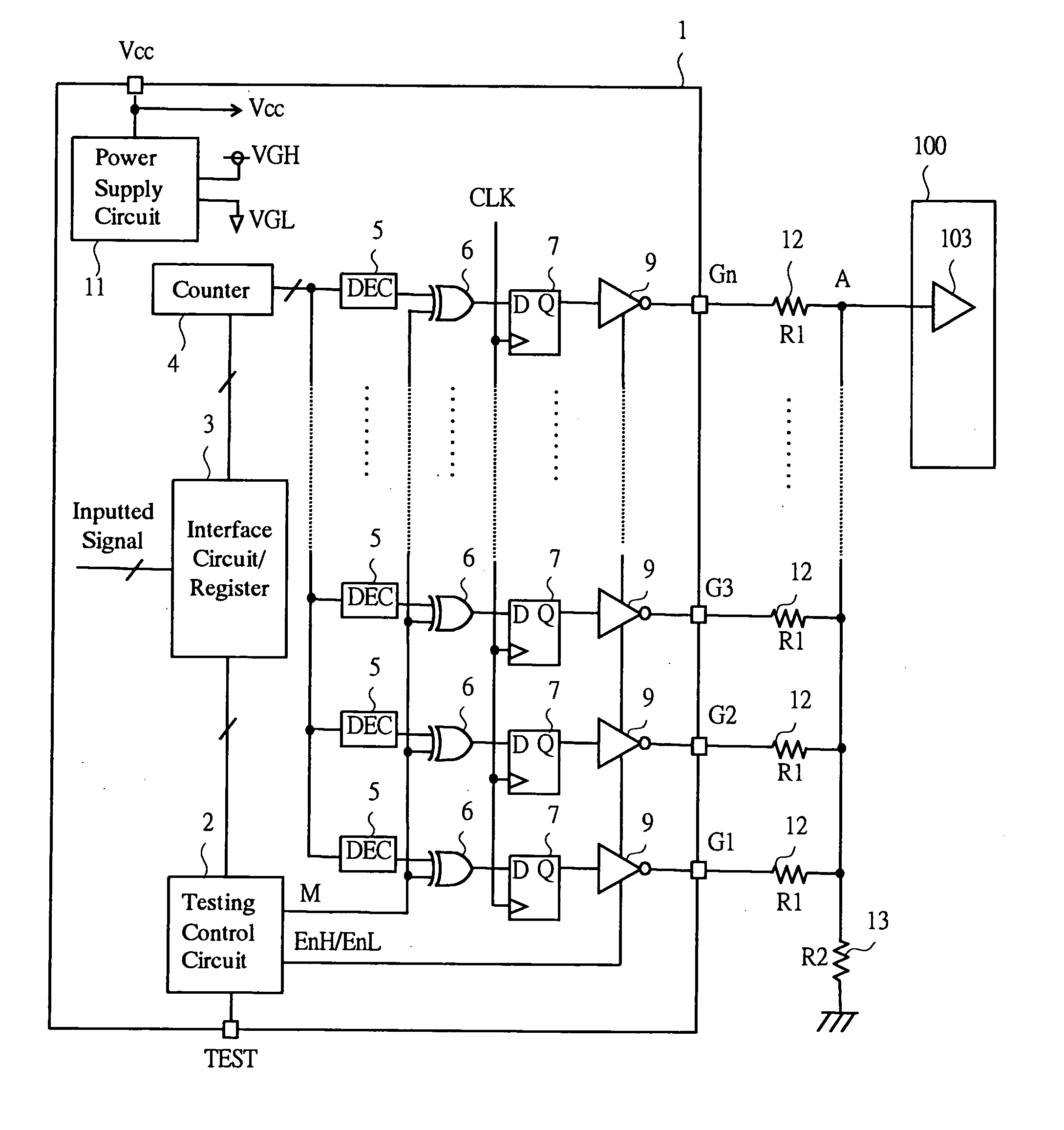
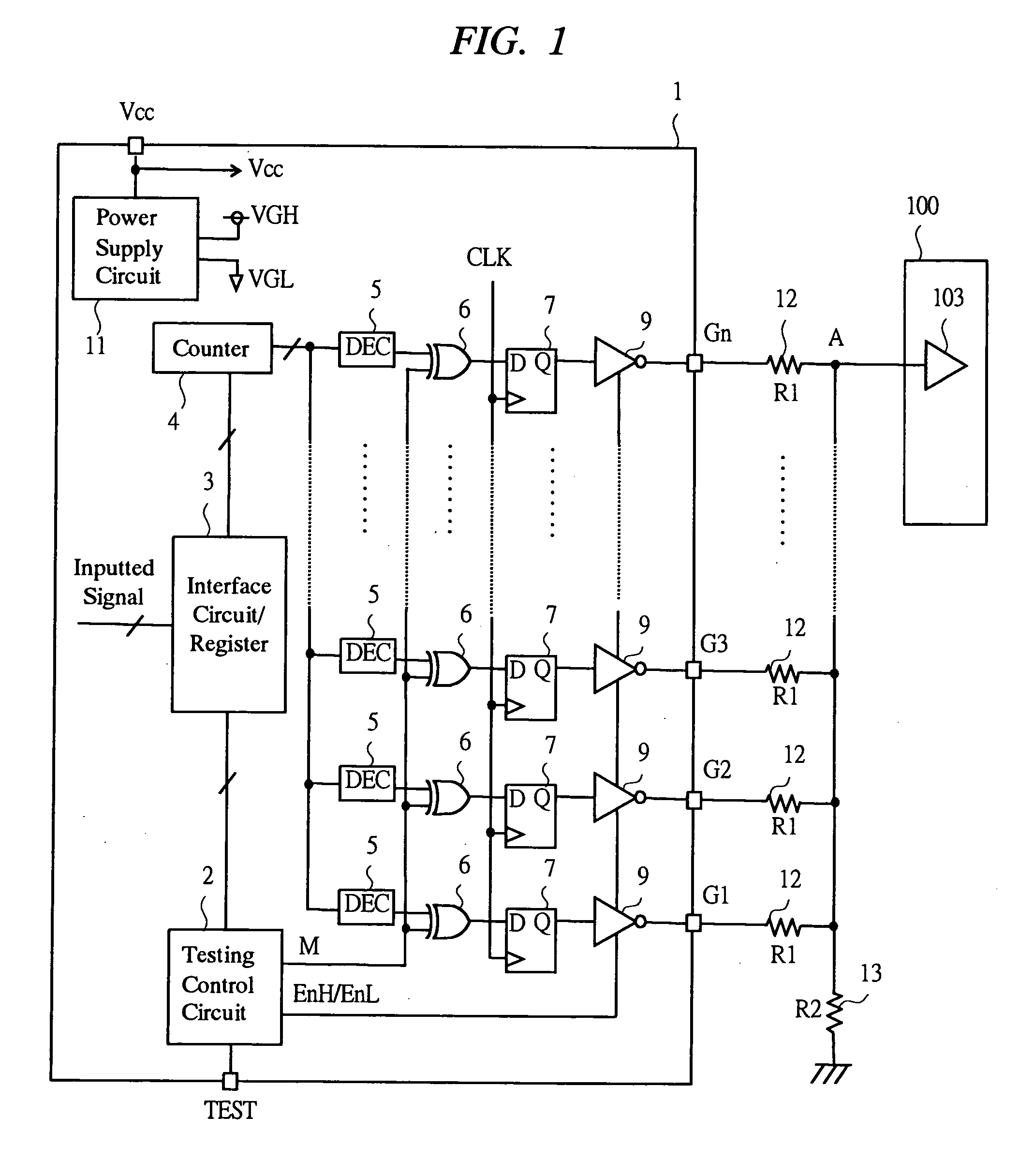
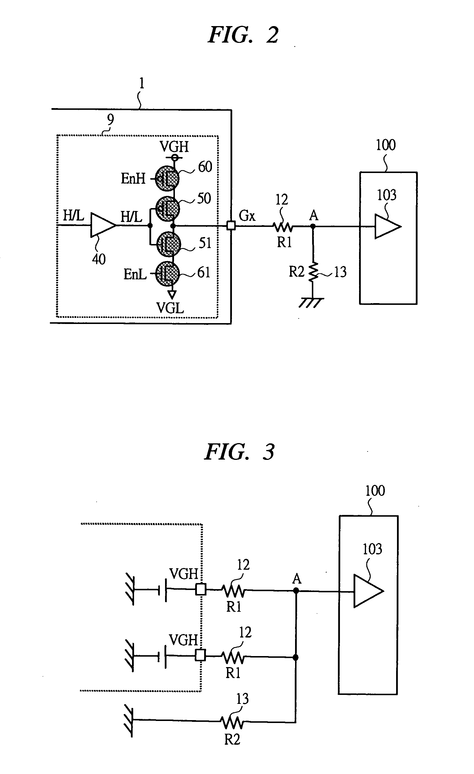
[0044] An LCD driver that is a first embodiment of a semiconductor device according to the present invention will be described using FIGS. 1 to 8. FIG. 1 is a view showing a configuration of an LCD driver; FIG. 2 is a view showing an equivalent circuit at a time of testing; FIG. 3 is a view showing an equivalent circuit at a time of assuming occurrence of failure; FIG. 4 is a view showing a setting state of a control signal; FIG. 5 is a view showing one example of a truth table of a test control circuit; FIG. 6 is a view showing an operation at a time of testing; FIG. 7 is a view showing a configuration example of an LCD driver having a small circuit scale; FIG. 8 is a view showing a circuit configuration of the inverter circuit in FIG. 7.

[0045] A LCD driver of a first embodiment is, as shown inFIG. 16 as described above, applied to the gate driver which is connected to the gate common terminal and has a function of executing the display control of the horizontal pixels, among the ...

second embodiment

[0069] An LCD driver, which is a second embodiment of a semiconductor device according to the present invention, will be described using FIGS. 9 to 12. FIG. 9 is a view showing a configuration of an LCD driver; FIG. 10 is a view showing an equivalent circuit at s time of testing; FIG. 11 is a view showing a configuration example of an LCD driver in which resetting of a reference voltage is not required; and FIG. 12 is a view showing a test pattern.

[0070] An LCD driver 1b of this embodiment represents, as shown in FIG. 9, one example in which the resistor network provided between the LCD driver and the semiconductor test equipment in the first embodiment is integrated into the LCD driver. It is provided with a switch (switch means) 17 which is connected to the first resistor 12 in series so as to separate the resistor network at a time of conducting no test. The description of setting each gate output voltage, each of the signals M, EnH, and EnL at the time of the testing (test mode...

third embodiment

[0078] An LCD driver, which is a third embodiment of a semiconductor device according to the present invention, will be described using FIGS. 13 and 14. FIG. 13 is a view showing a configuration of an LCD driver; and FIG. 14 is a view showing an equivalent circuit at a time of the testing.

[0079] A difference between an LCD driver 1d of a third embodiment and the LCD driver of the first embodiment is, as shown in FIG. 13, a configuration of the resistor network provided between the respective gate output terminals G1 to Gn and the semiconductor test equipment 100. Specifically, the first resistors 12 are connected between the respective gate output terminals, and one end (connecting point “A”) of the first resistor 12 connected only to the gate output terminal is terminated on the second terminal 13 by connecting the resistor network other than that of the first embodiment, the test mode (1) described in the first embodiment is set to conduct the test.

[0080] In this embodiment, the...


PUM


Abstract

A problem, which one of the inventions included in the present application solves, is to provide a semiconductor device that can simultaneously test a plurality of output pins by less channels of a semiconductor test equipment in number than the integrated output pins of the semiconductor device. Representative one of the inventions has such a configuration that an LCD driver, which is the semiconductor device having a function of driving a gate line of a liquid crystal display panel, comprises: an exclusive-OR circuit for inverting polarities of positive and negative voltages for driving the gate line; a tri-state type inverter circuit capable of changing and controlling, to a high-impedance state, an output circuit for driving the gate line; and at least one of test control terminals TEST for controlling the exclusive-OR circuit and the tri-state type inverter circuit. When a test is conducted, only one terminal of the gate output outputs a positive voltage VGH or negative voltage VGL and the other terminal is set to a high-impedance state, whereby the plurality of gate outputs are simultaneously tested.

Description

CROSS-REFERENCE TO RELATED APPLICATION [0001] The present application claims priority from Japanese patent application No. JP 2003-404691 filed on Dec. 3, 2003 and No. JP 2004-338903 filed on Nov. 24, 2004, the contents of which are hereby incorporated by reference into this application. BACKGROUND OF THE INVENTION [0002] The present invention relates to a semiconductor device and a testing method thereof and, especially, to a technique effectively applied to both of a semiconductor device such as a LCD driver having a function of driving gate lines of a liquid crystal display panel and a testing method thereof. [0003] Techniques that the inventors of the present invention have examined on the premise of the present invention will be described using FIGS. 16 to 19. FIG. 16 is a view showing a connection relation between a liquid crystal display panel and a LCD driver; FIG. 17 is a view showing a connection relation between a LCD driver and a semiconductor test equipment; FIG. 18 is ...

Claims


Application Information

Patent Timeline
IPC IPC(8): G02F1/1345G01R31/28G09G3/00G09G3/20G09G3/36
CPCG09G3/006G09G2310/0289G09G3/3677
Inventor IMAGAWA, KENGOMAKUUCHI, MASAMICHUJO, NORIOORIHASHI, RITSUROARAI, YOSHITOMO
Owner RENESAS ELECTRONICS CORP
Why Eureka
Try Eureka