Field programmable gate array incorporating dedicated memory stacks

a technology of dedicated memory and gate array, which is applied in the field of electronic modules, can solve the problems of limiting the usefulness of these devices, fpgas are typically designed, and a large amount of space on the printed circuit board is required

Inactive Publication Date: 2005-06-09
NYTELL SOFTWARE LLC
View PDF2 Cites 5 Cited by
  • Summary
  • Abstract
  • Description
  • Claims
  • Application Information

AI Technical Summary

Problems solved by technology

Not withstanding the great utility of FPGAs, there exist several limitations to the usefulness of these devices.
As suggested by FIG. 1, one of the limitations is that FPGAs are typically designed based on a design rule that assumes a fixed and limited word width which is particularly limiting when used in combination with a large amount of memory in high performance applications such as data processing and networking.
Further, when the FPGA is used to read from and write into a memory array that is arranged in a typical planar fashion, a considerable amount of space on the printed circuit board is required in order to physically provide for the combination of the FPGA and the memory.
Even when space is available for a large planar area that supports the FPGA and surrounding memory, large areas inherently increase parasitics and degrade performance.

Method used


Image

  • Field programmable gate array incorporating dedicated memory stacks
  • Field programmable gate array incorporating dedicated memory stacks
  • Field programmable gate array incorporating dedicated memory stacks

Examples


Embodiment Construction

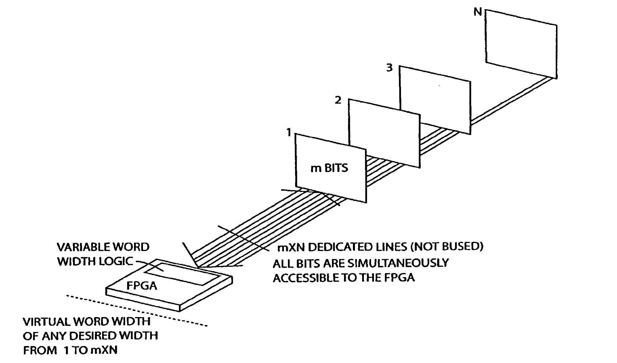
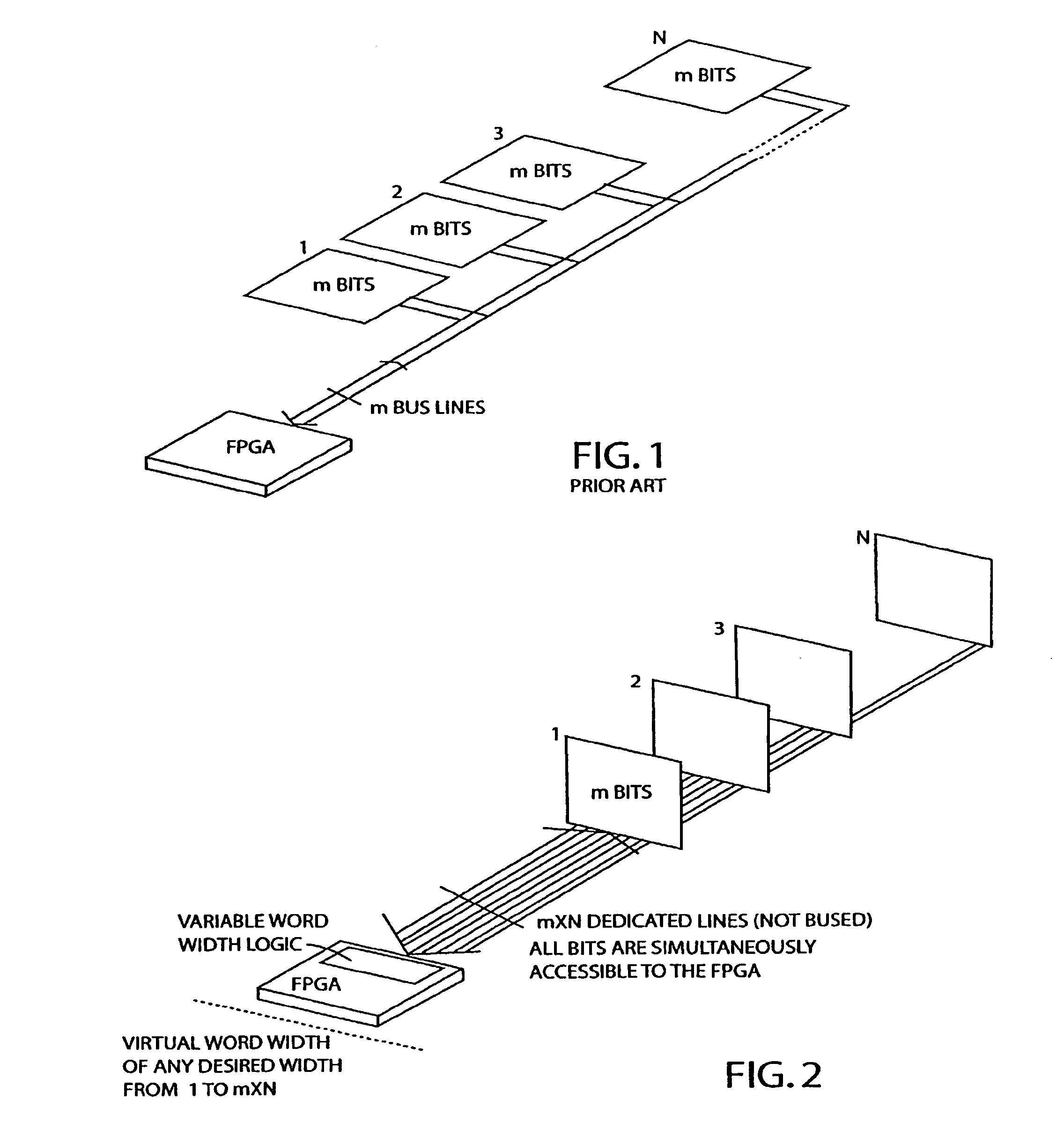
[0025]FIG. 2 is an simplified schematic view of a memory enhanced gate array according to a generalized embodiment of this invention a field programmable gate array (FPGA) has simultaneous access to all memory bits such that the FPGA, incorporating suitable logic, can implement a virtual word with of any desired width from 1 to m.times.N bits. Various particular embodiments are possible, two of which will now be discussed.

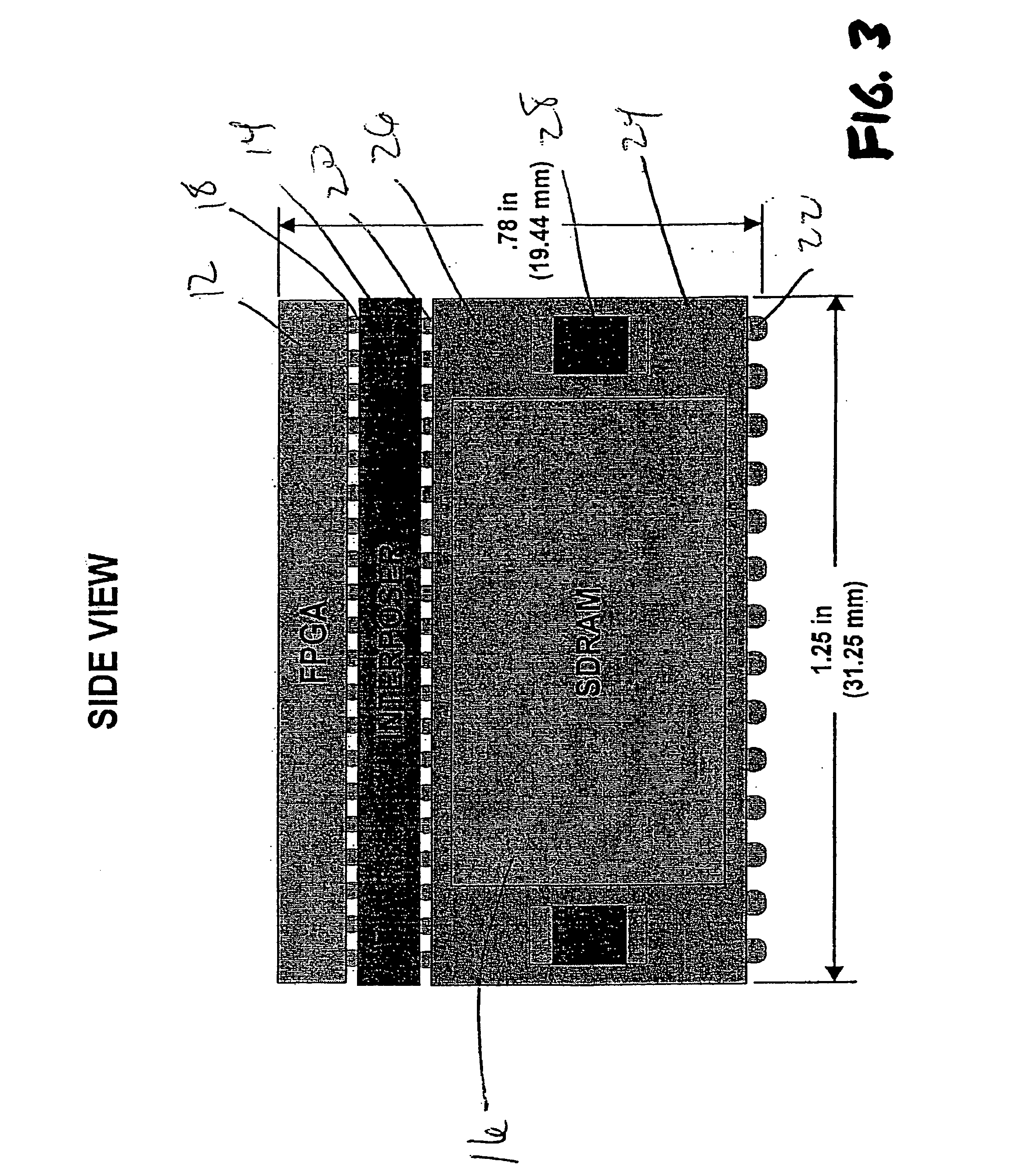
[0026]FIGS. 3 and 4 relate to a first preferred embodiment where an FPGA is coupled to an access lead network formed, in this particular case, by a proximate interposer board and a first ball grid array. A plurality of memories are coupled to the proximate interposer board through a second ball grid array. As discussed above, the FPGA operates with a variable word width. The plurality of memories are stacked to form a memory block. Each individual access lead to the memory in each layer of the memory stack is brought to the edge of the stack. Therefore, the FPGA c...


PUM


Abstract

A field programmable gate array, an access lead network coupled to the FPGA, and a plurality of memories electrically coupled to the access lead network. The FPGA, access lead network, and plurality of memories are arranged and configured to operate with a variable word width, namely with a word width between 1 and a maximum number of bits. The absolute maximum word width may be as large as m.times.N where m is the number of word width bits per memory chip and N is the number of memory chips.

Description

RELATED APPLICATIONS [0001] The present application is a continuation application of U.S. patent application Ser. No. 10 / 347,038, “Field Programmable Gate Array With A Variably Wide Word Width Memory”, filed Jan. 17, 2003, now allowed, which in turn is related to U.S. Provisional Patent Application Ser. No. 60 / 384,582, filed on Jan. 17, 2002, which is incorporated herein by reference and to which priority is claimed pursuant to 35 USC 119. BACKGROUND OF THE INVENTION [0002] 1. Field of the Invention [0003] The invention relates to an electronic module and in particular to a combination of a memory array with a field programmable gate array. [0004] 2. Description of the Prior Art [0005] Of the many varieties of integrated circuits available on the market today, field programmable gate arrays (FPGAs) are particularly useful when building many kinds of electronic devices and systems. Because FPGAs allow the designer to integrate complex logic that is peculiar to his application in one ...

Claims


Application Information

Patent Timeline
Patent Type & Authority Applications(United States)
IPC IPC(8): G01R31/3185G06F9/38H03K19/177
CPCG01R31/318519G06F9/3802H03K19/17796H03K19/1776H03K19/1778H03K19/17736H01L2224/16227H01L2924/15311
Inventor CARLSON, RANDOLPH STUARTOZGUZ, VOLKANGANN, KEITH D.LEON, JOHN P.
Owner NYTELL SOFTWARE LLC
Why Eureka
Try Eureka