Fingerprint reading device and personal verification system

Inactive Publication Date: 2005-06-09
CANON KK
8 Cites 71 Cited by

AI-Extracted Technical Summary

Problems solved by technology

As a technique of computerization of this personal verification, the method of inputting the image of a fingerprint has been in heavy usage, while, for example, a device using a total reflection prism as disclosed in Japanese Patent Application Laid-Open No. 2000-11142, which is a Japanese Patent, has been bristled with difficulties that its shape becomes large, and moreover, it is unable to discriminate a false fingerprint molded by resin and the like.
However, in this system, the light from the LED cannot be effectively used.
However, to obtain a sharp image, the thickness t of the cover glass 50 is required to be extremely thin, and to sidestep this requirement, it has been necessary to use an expensive material such as a fiber optics plate (FOP) and the like.
H10-222641, although a structure being superposed up and down with a linear image pickup element, a linear light source havin...

Benefits of technology

[0031] According to the present invention, the light irradiating means constituted by a plurality of LEDs and the like is placed side by side with the imaging means, and the light irradiating means is arranged along the length more than the reading effective length in the main scanning direction along at least the main scanning direction of t...

Abstract

An influence by a light quantity distribution of light irradiating means in a fingerprint image is decreased, so that an excellent fingerprint image improved in contract can be obtained. Light irradiating means for irradiating a light on a finger arranged on a predetermined region, and a solid state image pickup element for receiving a diffused light from the inside of the finger by the light irradiated from this light irradiating means and for picking up the fingerprint image of the finger is provided, and the light irradiating means is arranged across a length at least equal to or more than an effective reading length (L) of the solid state image pickup element.

Application Domain

Technology Topic

Image

  • Fingerprint reading device and personal verification system
  • Fingerprint reading device and personal verification system
  • Fingerprint reading device and personal verification system

Examples

  • Experimental program(3)

Example

First Embodiment
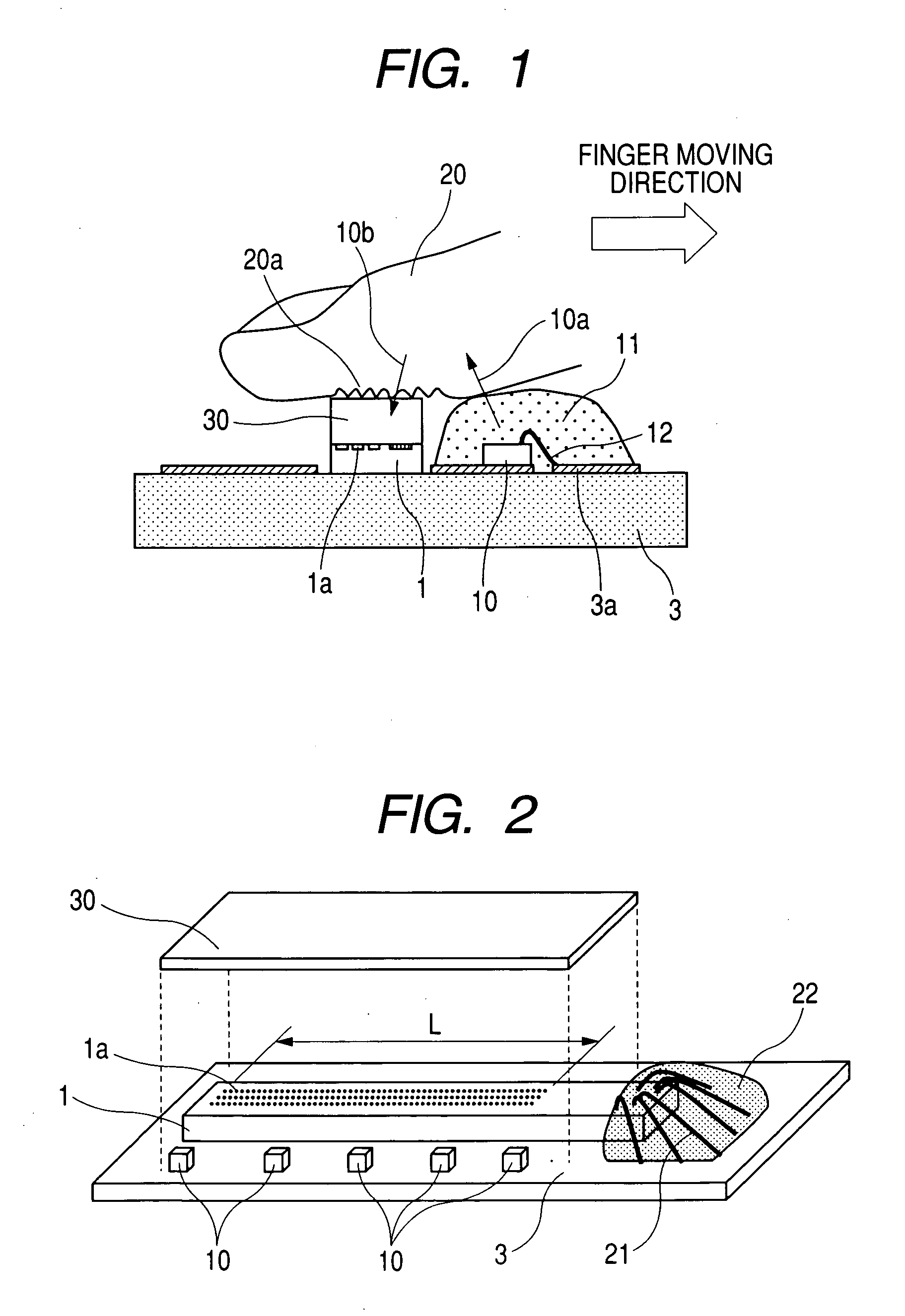
[0048]FIG. 1 is a schematic sectional view of the fingerprint reading device in a first embodiment of the present invention. Further, FIG. 2 is an oblique view of the fingerprint reading device in the first embodiment of the present invention.
[0049] In the fingerprint reading device shown in FIGS. 1 and 2, a solid state image pickup substrate 1 and a LED chip 10 are arranged on a wiring substrate 3. The solid state image pickup substrate 1 is mounted with a plurality of solid state image pickup elements 1a arranged in a line. A LED chip 10 has a LED which is light irradiating means for irradiating at least either one from among an infrared light and a near infrared light.
[0050] The solid state image pickup substrate 1, as shown in FIG. 2, has an electrode unit arranged at an end portion in a longitudinal direction electrically connected to a wiring 3a on a wiring substrate 3 by a wire 21. Similarly, the LED chip 10 has its electrode unit also electrically connected to the wiring 3a on the wiring substrate 3 by the wire 12. In the solid state image pickup substrate 1, a protective layer 30 is arranged on the reading surface to which a finger 20 contacts. As a material of the protective layer 30, glass, a SiO2 thin film, a SiON thin film, a fiber optical plate and the like can be used. These materials are adhered on the solid state image pickup element 1a of the solid sate image pickup substrate 1 by a bonding agent which transmits the infrared light and the near infrared light.
[0051] The protective layer 30 is required to satisfy the following each item to be able to have a still lower price and to read a detailed image. [0052] 1. When considering the filtering out of the light (cross talk) into adjacent solid state image pickup elements, a refraction factor has to be high to suppress the spread of the light between incidence and emission. [0053] 2. An unnecessary light other than the irradiating light is not to be incident to obtain a sharp image. [0054] 3. To have abrasion-proof and weatherproof. [0055] 4. To be at a low cost. [0056] 5. To have easy workability. [0057] 6. When considering bowing and deformation, coefficient of linear expansion has to be close to the solid state image pickup substrate 1.
[0058] To satisfy the above requirements, a silicon substrate is particularly suitable. The silicon substrate is workable to attain a desired thickness by back grinding or back lapping. Further, since the silicon substrate transmits the infrared light and the near infrared light and cuts a visible light, it can cut an unnecessary light such as an external light. Since its refraction factor is also about 3.4, even when it has a thickness 1.5 to 2 times that of glass, it can obtain an equivalent resolution. In case the silicon substrate is used as the protective layer 30, the substrate having thicknesses from 30 μm to 200 μm is usable, and particularly, the thicknesses from 70 μm to 150 μm are suitable.
[0059] Further, as shown in FIG. 2, the solid sate imaging pickup element 1a has a reading effective length L in the main scanning direction (horizontal direction) formed in 15 mm. Further, a LED column which is the light irradiating means is constituted by five pieces of the LED chip 10, and the LED column is arranged in the range equal to or more than the reading effective length L of the solid state image pickup element.
[0060] Here, in the fingerprint reading device of the present embodiment, the light quantity distribution by the light irradiating means at the main scanning direction (horizontal direction) in the solid state image pickup element 1a is studied. FIG. 3 is a characteristic view showing the light intensity in the horizontal direction position in the solid state image pickup element 1a. In FIG. 3, a solid line 60 denotes the light intensity in an adjacent state of the LED column, which is the light irradiating means, to the finger. Further, as a reference, the light intensity in case the light irradiating means is installed 1 mm spaced away from the finger is shown in a broken line 61. Further, the effective reading length of the solid state image pickup element 1a is a length shown in reference numeral 63. Granted that the solid state image pickup element 1a have in its outside most dummy pixels and the like which do not read an OB pixel and an image, those are naturally not taken into consideration as falling under the reading effective length. The installing position of the LED chip 10 used as the light irradiating means is shown in a square 62 under the graph.
[0061] The characteristic view shown in FIG. 3 shows the light intensity in case a sub scanning direction (vertical direction) distance with the solid state image pickup element 1a and the light irradiating means is about 1.5 mm. The characteristic shown by the solid line 60 is such that, since the finger is closely adhered to the light irradiating means, the light diffusion between the solid state image pickup element 1a and each light source 62 of the light irradiating means does not sufficiently proceed, so that the distribution of the light intensity in the solid state image pickup element 1a remains large. Further, by installing the light irradiating means isolated from a state of closely adhering to the finger, the change of the light intensity can be improved. However, that light intensity ends up being reduced to about one third as compared to the case where the light irradiating means is closely adhered to the finger.
[0062] In the meantime, FIG. 4 is a characteristic view showing the light intensity in case the light irradiating means is isolated about 2.5 mm from the sub scanning direction (vertical direction). In this case, even while the light irradiating means remains in a state of adhering to the finger, it will be appreciated that sufficiently uniformized light intensity can be obtained in the effective reading length 63 of the solid state image pickup element 1a.
[0063] Further, FIG. 5 is a characteristic view showing the light intensity in case the range of the irradiating means is set shorter than the effective reading length 63 of the solid state image pickup element 1a. As evident from FIG. 5, the light intensity within the effective reading length 63 of the solid state image pickup element 1a is observed to be attenuated at both end portions of the effective reading length 63, so that uniformity of sufficient light intensity is not obtained. Further, FIG. 6 is a characteristic view showing the light intensity in case the light irradiating means is isolated about 2.5 mm from the solid state image pickup element 1a in the sub scanning direction (vertical direction) and the length in which the light irradiating means is arranged is set longer than the effective reading length 63 of the solid state image pickup element 1a. As evident from FIG. 6, in this case, uniformity of sufficient light intensity can be obtained within the effective reading length 63 of the solid state image pickup element 1a.
[0064] In the sweep type adjacent optical fingerprint reading device, in the case of the present embodiment, when the distance of the sub scanning direction (vertical direction) with the solid state image pickup element 1a and the LED column of the light irradiating means is, in consideration of the miniaturization, preferably set in the range of about 1.6 mm to 3.0 mm, and more preferably set in the range of about 2.0 mm to 2.5 mm, the influence of the solid state image pickup element 1a to the distribution of the light intensity in the LED light source can be decreased.
[0065] Although each LED chip 10 used in the LED column, which is the light irradiating means, is preferably all alike in its light output, in the actual LED chip 10, the light output has variation even in the same input current. Uniformity of the irradiating light in the present embodiment, when considering the influence toward a recognition rate of the fingerprint reading device generally required by its output image, is preferably about 20% as a light quantity distribution, and moreover, is required to be within 15% in case an accuracy is demanded. To maintain such uniformity of the irradiating light, variation of the light output of each LED chip 10 is also preferably within about 20%. Moreover, although the LED chips 10 are preferably lined up at equal intervals for the effective reading length L of the solid state image pickup element 1a, the intervals may be approximately the same.
[0066] Consequently, according to the present embodiment, by arranging the LED column in the LED chip 10 in the range equal to or more than the effective reading length L of the solid state image pickup element 1a, the influence by the light quantity distribution of the light irradiating means in the input fingerprint image of the fingerprint reading device can be decreased. Further, by using a silicon substrate as a thin film filter, an excellent fingerprint image improved in contrast and at a low cost can be obtained.

Example

Second Embodiment
[0067]FIG. 7 is a schematic sectional view of a fingerprint reading device in a second embodiment of the present invention. Further, FIG. 8 is an oblique view of the fingerprint reading device in the second embodiment of the present invention.
[0068] While the fingerprint reading device in the second embodiment shown in FIGS. 7 and 8 has entirely the same constitution as the fingerprint reading device (see FIGS. 1 and 2) of the first embodiment, moreover, LED columns constituting light irradiating means are formed both up and down of a sub scanning direction (vertical direction) in a solid state image pickup element 1a. That is, the LED column of the present embodiment, as shown in FIG. 8, has a LED chip 10 arranged in a wiring substrate3 similarly to the first embodiment and its electrode unit is formed by being electrically connected to a wiring portion of a wiring substrate 3 by a wire 12, and at the same time, a second LED column constituted by LED chips 13 is formed above for the sub scanning direction in the solid state image pickup element 1a. The LED chips 13 constituting this second LED column have the same number of LEDs as the first LED column, and are provided on the wiring substrate 3 at equal chip intervals.
[0069] Consequently, according to the present embodiment, in addition to the advantage in the first embodiment, the light quantity change in the sub scanning direction in the solid state image pickup element 1a can be further reduced.
[0070] In the sweep type fingerprint device, an image inputting of the entire finger is not performed, but a partial image of the finger to be scanned is taken, and from the characteristic point of each image, the fingerprint image has to be reconstituted. Hence, a continuity of the partial images to be used for image reconstitution is important. In practice, the light quantity change of the sub scanning direction of the solid state image pickup element 1a is important. In the partial images to be used for image reconstitution, the light quantity change of the sub scanning direction harms the continuity of the partial images obtained. Hence, in the fingerprint reading device of the second embodiment, since the continuity of the partial images of the fingerprint image inputted from the solid state image pickup element 1a is easily secured, a deficiency of partial images when reconstituting the entire fingerprint image does not develop, and moreover, accuracy of the obtained reconstituted image is high, so that a recognition rate in the fingerprint verification system using the fingerprint reading device of the present embodiment can be improved.

Example

Third Embodiment
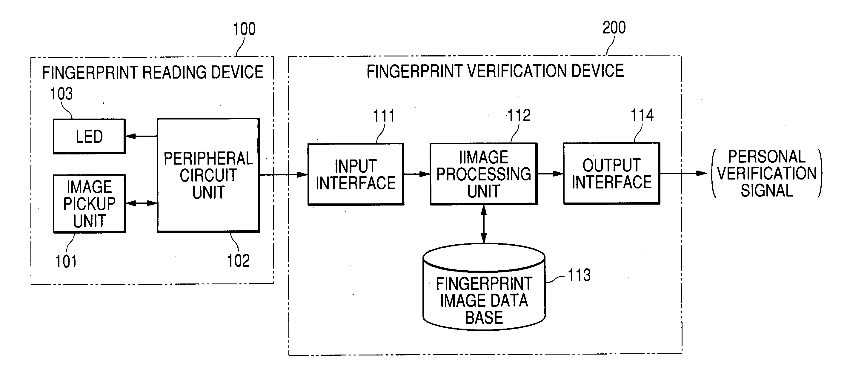
[0071] Next, an embodiment of a personal verification system including the above described fingerprint reading device will be described with reference to FIGS. 9 and 10.
[0072]FIG. 9 is a schematic block diagram of a personal verification system in a third embodiment of the present invention. Further, FIG. 10 is a schematic block diagram of a fingerprint reading device 100 constituting the personal verification system in the third embodiment.
[0073] The personal verification system shown in FIG. 9 comprises: the fingerprint reading device 100 comprising an image pickup unit 101 constituted by a solid state imaging senor 1a, a peripheral circuit unit 102 thereof, and a LED 103 mounted in a LED chip 10; and a fingerprint verification unit 200 which is connected to the fingerprint reading device 100 and performs a fingerprint verification.
[0074] The peripheral circuit unit 102, for example, is formed on a solid state image pickup element substrate 1, and as shown in FIG. 10, is constituted by including a control circuit (drive circuit) 1021 for controlling the operation of a solid state image pickup unit 101, an A/D converter 1023 for converting an analogue imaging signal corresponding to an image related to the finger pattern of a finger outputted from the image pick up unit 101 from an analogue signal to a digital signal through a clamp circuit 1022, a communication control circuit 1024 and a register 1025 connected to thereof for performing a data communication of the digital signal converted by the A/D converter 1023 as an image signal of the fingerprint for an external device (interface and the like), a LED control circuit 1026 for controlling the emission of the LED of the LED 103, and a timing generator 1028 for generating a control pulse for controlling the operation timing of the above described circuits 1021 to 1026 based on a reference pulse provided from an external oscillator 1027. The circuits including this peripheral circuit 102 are not limited to the above described circuits, but may include different types of circuits. Further, a portion of the above described circuits may be constituted as a different chip.
[0075] A fingerprint verification device 200 comprises: an input interface 111 for inputting a communication data outputted from the communication control unit 1024 of the peripheral circuit unit 102; an image processing unit (fingerprint verification means) 112 connected to this input interface 111; and a fingerprint image data base (fingerprint registration means) 113 connected to this image processing unit 112; and an output interface 114. The output interface 114 is connected to electronic equipment (including software also) required for the personal verification in order to ensure security and the like at the time of usage and login.
[0076] Here, a fingerprint image data base 113 is registered with a fingerprint image of the finger of an object individual to be individually certified in advance. The object individual here may be one or a plurality of individuals. The fingerprint image of the object individual is inputted from the fingerprint reading device 100 as the personal verification information of the object individual through the input interface 111 at an initial set-up time, an object individual adding time, and the like.
[0077] The image processing unit 112 inputs the fingerprint image read by the fingerprint reading device 100 through the input interface 111, and verifies whether or not the read fingerprint image matches the registered image of the fingerprint image data base 113 based on a known fingerprint verification image processing algorism, and outputs its verification result (fingerprint matches or does not match) as a personal verification signal through the output interface 114.
[0078] In the present embodiment, although the fingerprint reading device 100 and the fingerprint verification device 200 are constituted by separate devices, the present invention is not limited to this, but as occasion demands, at least a part of functions of the finger verification device 200 may be integrally constituted within the peripheral circuit 102 of the fingerprint reading device 100. Further, the personal verification system of the present embodiment may be integrally assembled and constituted within the electronic equipment required for the personal verification or may be constituted by a separate unit from the electronic equipment.
[0079] According to the present embodiment of the present invention, for the effective reading length of the solid state image pickup element 1a, the light irradiating means is arranged at the same position as both ends of the reading length or up to the outside position of that length, so that the irradiating light quantity distribution of the solid state image pickup element 1a can be easily improved, and an uniform light quantity by the light irradiating means can be obtained as shown in FIG. 11. Hence, the changed portion only of the output by the fingerprint pattern is enlarged from the output of the solid state image pickup element 1a, thereby improving the contrast and inputting an excellent fingerprint image.
[0080] This application claims priority from Japanese Patent Application No. 2003-408992 filed Dec. 8, 2003, which is hereby incorporated by reference herein.

PUM

no PUM

Description & Claims & Application Information

We can also present the details of the Description, Claims and Application information to help users get a comprehensive understanding of the technical details of the patent, such as background art, summary of invention, brief description of drawings, description of embodiments, and other original content. On the other hand, users can also determine the specific scope of protection of the technology through the list of claims; as well as understand the changes in the life cycle of the technology with the presentation of the patent timeline. Login to view more.

Similar technology patents

Liquid crystal compound and liquid crystal composition containing same, and liquid crystal display device

PendingCN113528152AWide Nematic Temperature RangeGood contrastLiquid crystal compositionsOrganic chemistryDielectric anisotropyRotational viscosity
Owner:JIANGSU HECHENG ADVANCED MATERIALS

Contrast Dyes for Inkjet Lithographic Printing Plates

InactiveUS20090036638A1Good contrastAzo dye preparationMonoazo dyesCarbon atomPhotochemistry
Owner:AGFA NV

Classification and recommendation of technical efficacy words

  • Good contrast
  • Reduce influence

Double-frequency laser interferometry apparatus

InactiveCN101413783AAvoid frequency aliasingGood contrastUsing optical meansOptical pathOpto electronic
Owner:BEIJING CHANGCHENG METERING TEST TECH INST NO 1 GRP CO CHINA AVIATION IND
Why Eureka
Try Eureka