

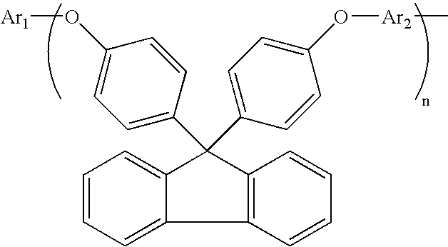
Novel poly(arylene ether) dielectrics
a dielectric and polymer technology, applied in the field of dielectric materials, can solve the problems of reducing the performance of the device, increasing the propagation delay, and reducing the power dissipation of the interconnect structure, so as to prevent undesirable diffusion
- Summary
- Abstract
- Description
- Claims
- Application Information
AI Technical Summary
Benefits of technology
Problems solved by technology
Method used
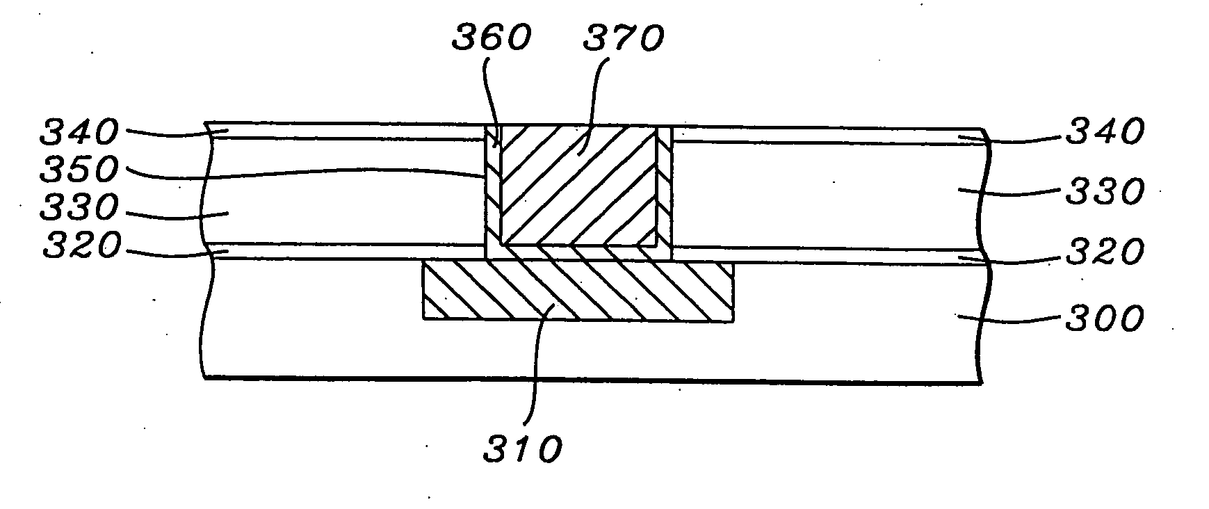
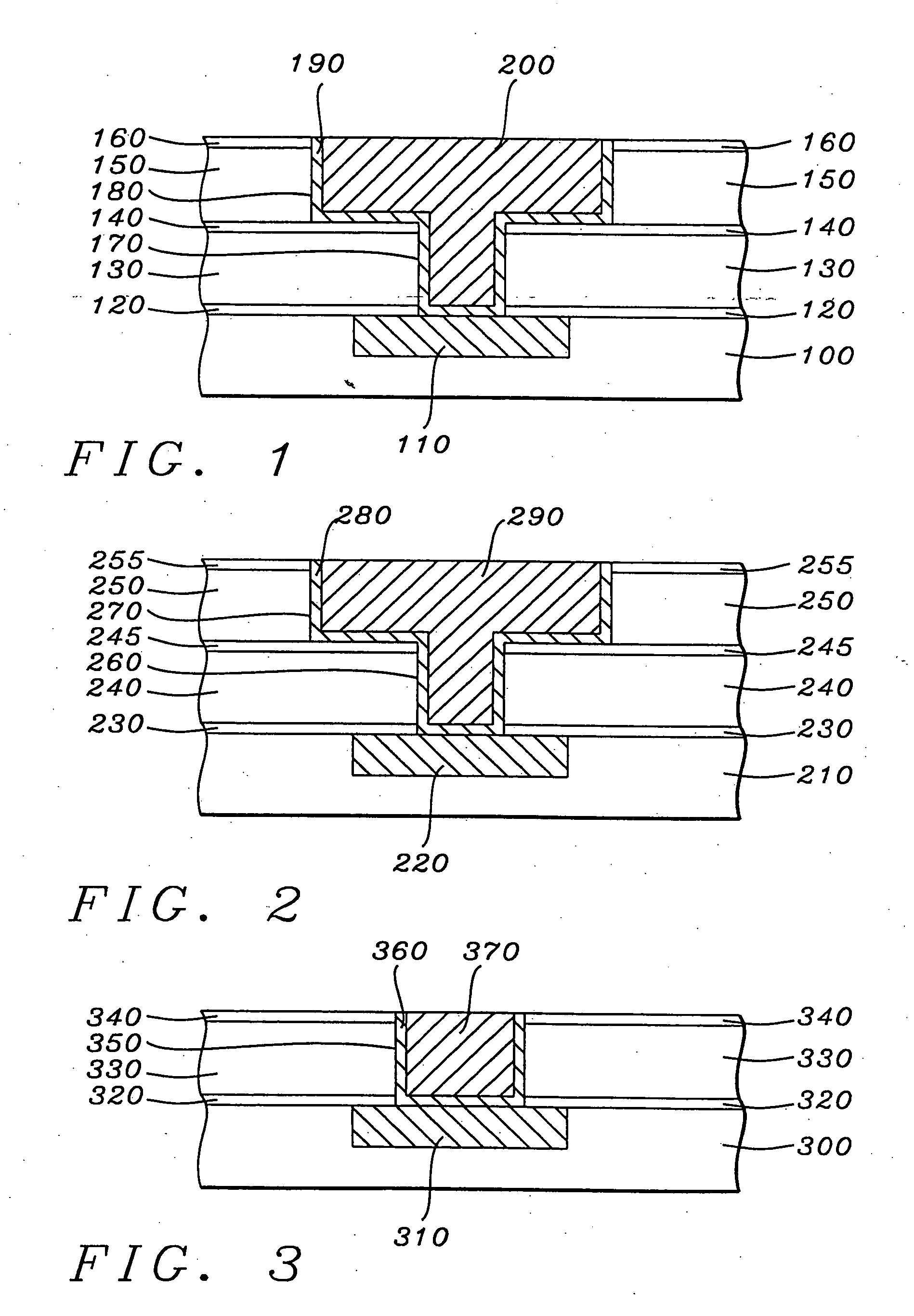
Image

Examples
example 1
Synthesis of Polymer “A”
[0049] In a 50 ml flask, 0.06 gm (0.61 mmol) of copper(l) chloride was added to 0.6 ml of quinoline contained under a nitrogen blanket. The mixture was stirred at 25° C. for 48 hours. A mixture of 1 gm (2.86 mmol) of 9,9bis(4-hydroxyphenyl)fluorene, 2.5 gm of toluene and 5 gm of benzophenone was charged to a 50 ml, 3-necked, round bottom flask fitted with a distillation set, magnetic stirrer and thermometer. The mixture was heated to 60° C. with stirring and in a nitrogen environment. After homogeneity had been reached, 0.263 gm (5.72 mmol) of aqueous sodium hydroxide solution was added dropwise to the mixture. A water azeotrope was then collected by vacuum distillation at an elevated temperature. After complete dehydration and removal of toluene, the reaction mixture was cooled to room temperature and the distillation set was replaced by a condenser. The reaction mixture was then heated to 80° C. and 0.69 gm (2.86 mmol) of 2,5-dibromothiophene was added. The...
PUM
| Property | Measurement | Unit |
|---|---|---|
| temperature | aaaaa | aaaaa |
| room temperature | aaaaa | aaaaa |
| diameter | aaaaa | aaaaa |
Abstract
Description
Claims
Application Information