Method of forming isolation film in semiconductor device

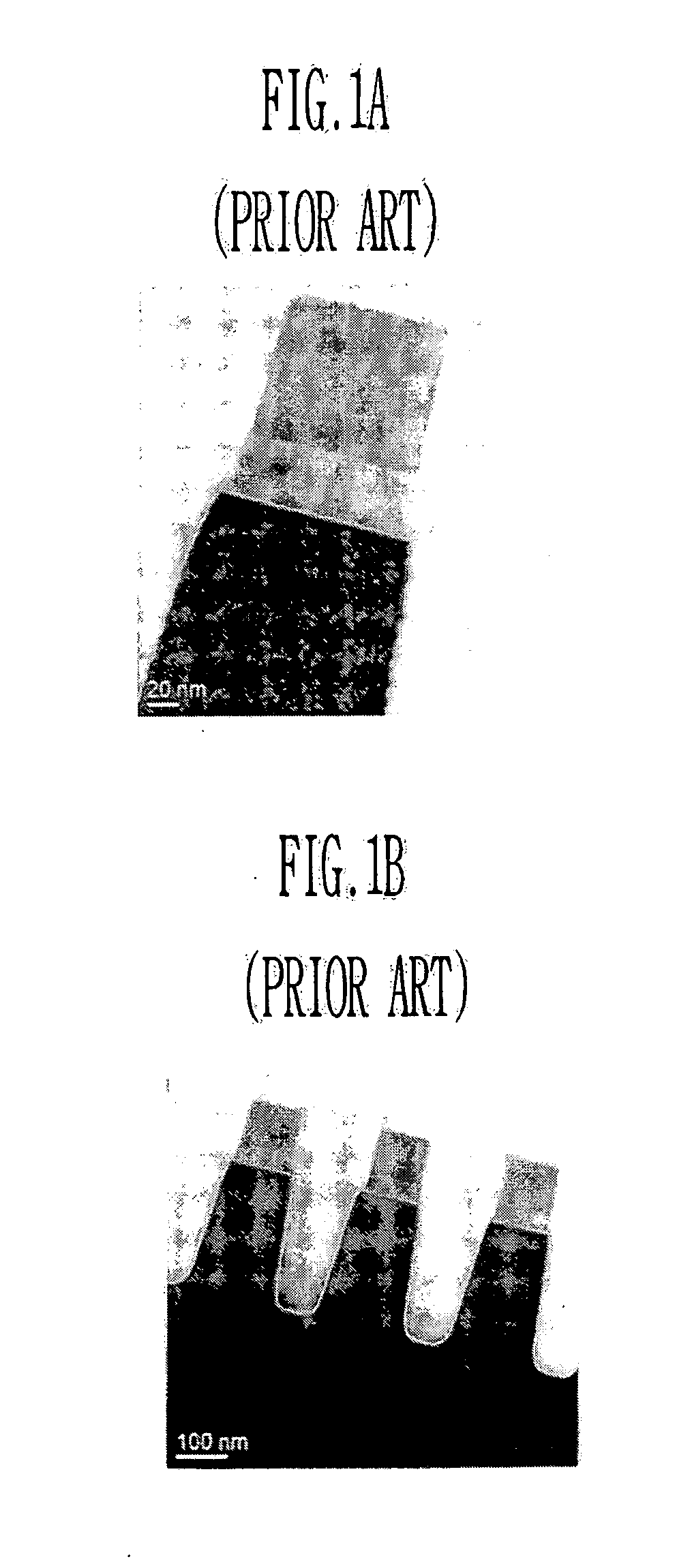
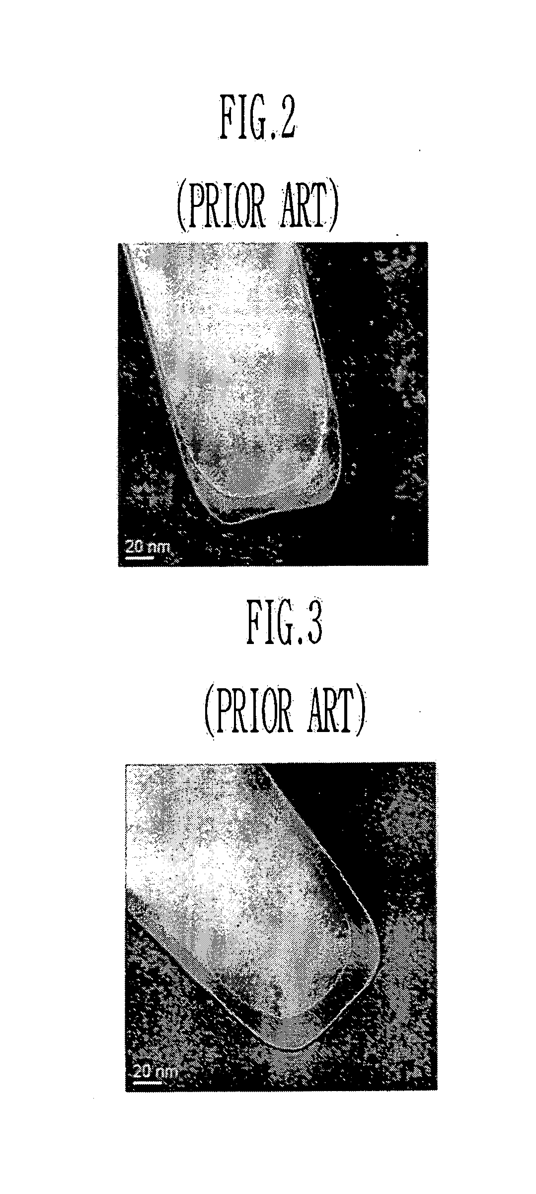
a technology of isolation film and semiconductor, applied in the direction of semiconductor devices, electrical devices, transistors, etc., can solve the problems of uneven oxidation, adversely affecting the properties of isolation film, damage to semiconductor substrates exposed to etching process, etc., and achieve the effect of improving the roughness of the trench sidewall

Active Publication Date: 2005-06-16
MICRON TECH INC +1
View PDF12 Cites 11 Cited by
  • Summary
  • Abstract
  • Description
  • Claims
  • Application Information

AI Technical Summary

Benefits of technology

[0014] The present invention is contrived to solve the aforementioned problems, and an object of the present invention is to provide a method for forming an isolation film in a semiconductor device wherein the roughness of a trench sidewall is improved by performing a predetermined cleaning process after a trench for isolation is etched and a uniform sidewall oxide film is formed as a PET process is omitted.

Problems solved by technology

At this time, an abnormal layer is formed due to polymer of a carbon series generated from the PET process, thus resulting in uneven oxidization in a subsequent oxidization process.
Referring to FIG. 1A and FIG. 1B, after a trench for isolation is formed, if a post cleaning process is performed, the semiconductor substrate exposed by the etch process is damaged.
Damage of the semiconductor substrate within the trench adversely affects the properties of the isolation film.
If the inside of the trench wherein the abnormal layer is formed is experienced by a sidewall oxidization process, a very uneven sidewall oxide film is formed.
Accordingly, there occurs a problem that a target trench shape is difficult to form.
It is also impossible to reduce damage due to the etch.

Method used


Image

  • Method of forming isolation film in semiconductor device
  • Method of forming isolation film in semiconductor device
  • Method of forming isolation film in semiconductor device

Examples


Embodiment Construction

[0026] Now the preferred embodiments according to the present invention will be described in detail with reference to the accompanying drawings. Since preferred embodiments are provided for the purpose that the ordinary skilled in the art are able to understand the present invention, they may be modified in various manners and the scope of the present invention is not limited by the preferred embodiments described later. Like reference numerals are used to identify the same or similar parts.

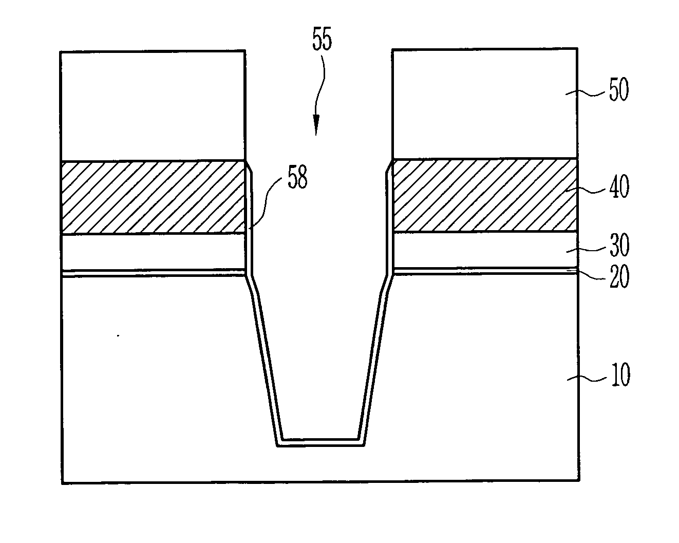
[0027]FIG. 5A to FIG. 5D are cross-sectional views illustrating a method for forming an isolation film according to the present invention.

[0028] Referring to FIG. 5A, an ion implantation process for forming a well and controlling the threshold voltage are performed on a semiconductor substrate 10, thus forming a well and an ion layer for controlling the threshold voltage (not shown). It is preferred that the well is a triple well including an N well and a P well.

[0029] A tunnel oxide film 20, ...


PUM


Abstract

The present invention relates to a method for forming an isolation film in a semiconductor device. After a trench for isolation is formed, a polymer film is stripped by a post cleaning process using BFN. A pre-treatment cleaning process using only SC-1 is performed and a sidewall oxidization process is then carried out. It is therefore possible to improve fail of the roughness of the trench sidewall and to easily strip polymer. Furthermore, since a conventional PET process is omitted, an isolation film manufacturing process is simplified. It is also possible to prohibit out-diffusion of dopants injected into a semiconductor substrate through a pre-treatment cleaning process using CLN N before the sidewall oxidization process. Incidentally, by forming a slope at the top corner of the trench, it is possible to prevent a gate oxide film thinning phenomenon that the gate oxide film thinner than a desired thickness is deposited at the trench corner. It is also possible to improve electrical properties of a device since an active region as much as a target critical dimension is secured.

Description

[0001] This application relies for priority upon Korean Patent Application No. 2003-0089983 filed on Dec. 11, 2003, the contents of which are herein incorporated by reference in their entirety. BACKGROUND [0002] 1. Field of the Invention [0003] The present invention relates to a method for forming an isolation film in a semiconductor device, and more specifically, to a method for forming a self-aligned shallow trench pattern in a NAND flash device. [0004] 2. Discussion of Related Art [0005] Generally, in order to form a transistor on a semiconductor substrate, an active region that is electrically electrified and an isolation region for preventing electrical electrification and isolating elements are formed in the semiconductor substrate. A portion of the semiconductor substrate in the isolation region is etched and is then filled to form an isolation film. [0006] Conventionally, after the semiconductor substrate in the isolation region is etched, a post etch treatment (PET) process...

Claims


Application Information

Patent Timeline
Patent Type & Authority Applications(United States)
IPC IPC(8): H01L21/306H01L21/308H01L21/76H01L21/762H01L21/8247H01L27/115H01L29/788H01L29/792
CPCH01L21/02052H01L21/3081Y10S438/906H01L27/115H01L27/11521H01L21/76224H10B69/00H10B41/30H01L21/76
Inventor DONG, CHA DEOKHAN, IL KEOUN
Owner MICRON TECH INC
Why Eureka
Try Eureka