Method for manufacturing a printed circuit board that mounts an integrated circuit device thereon and the printed circuit board

Inactive Publication Date: 2005-06-23
BROTHER KOGYO KK
View PDF3 Cites 2 Cited by
  • Summary
  • Abstract
  • Description
  • Claims
  • Application Information

AI Technical Summary

Benefits of technology

[0006] Lands for being connected or bonded to each of the pins of the semiconductor on a printed circuit board are normally plated. In view of reducing manufacturing costs, electrolytic plating is generally applied to the lands due to its high-speed plating. When electrolytic plating is performed for the lands on the printed circuit board, a predetermined voltage has to be applied individually to all the lands that are to be connected or bonded to the pins of the semiconductor. To apply the voltage, a plurality of terminals has to be precisely made to contact with each of the lands, which leads to a

Problems solved by technology

Semiconductor devices are becoming smaller in size, due to demands to downsize electronic apparatuses.
As a semiconductor device is further miniaturized with its pins provided at a narrower pitch, a probe of a tester will accidentally contact pins other than a particular pin of the semiconductor device mounted on a printed circuit board when the device is tested.
To apply the voltage, a plurality of terminals has to be precisely made to contact with each of the lands, which leads to a complicated plating mechanism.
Further, it

Method used


Image

  • Method for manufacturing a printed circuit board that mounts an integrated circuit device thereon and the printed circuit board
  • Method for manufacturing a printed circuit board that mounts an integrated circuit device thereon and the printed circuit board
  • Method for manufacturing a printed circuit board that mounts an integrated circuit device thereon and the printed circuit board

Examples


Embodiment Construction

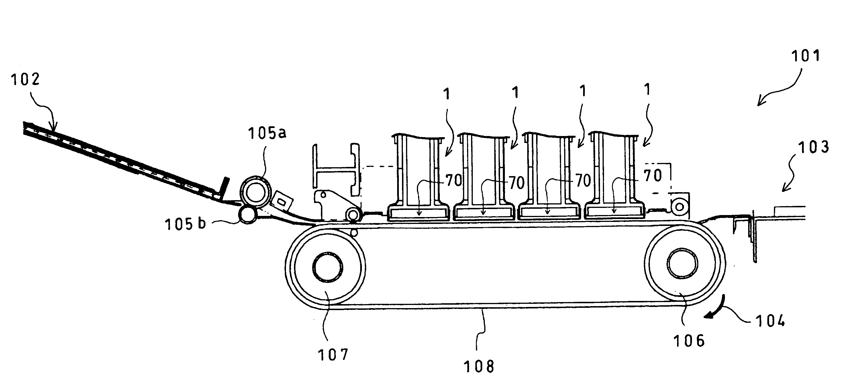
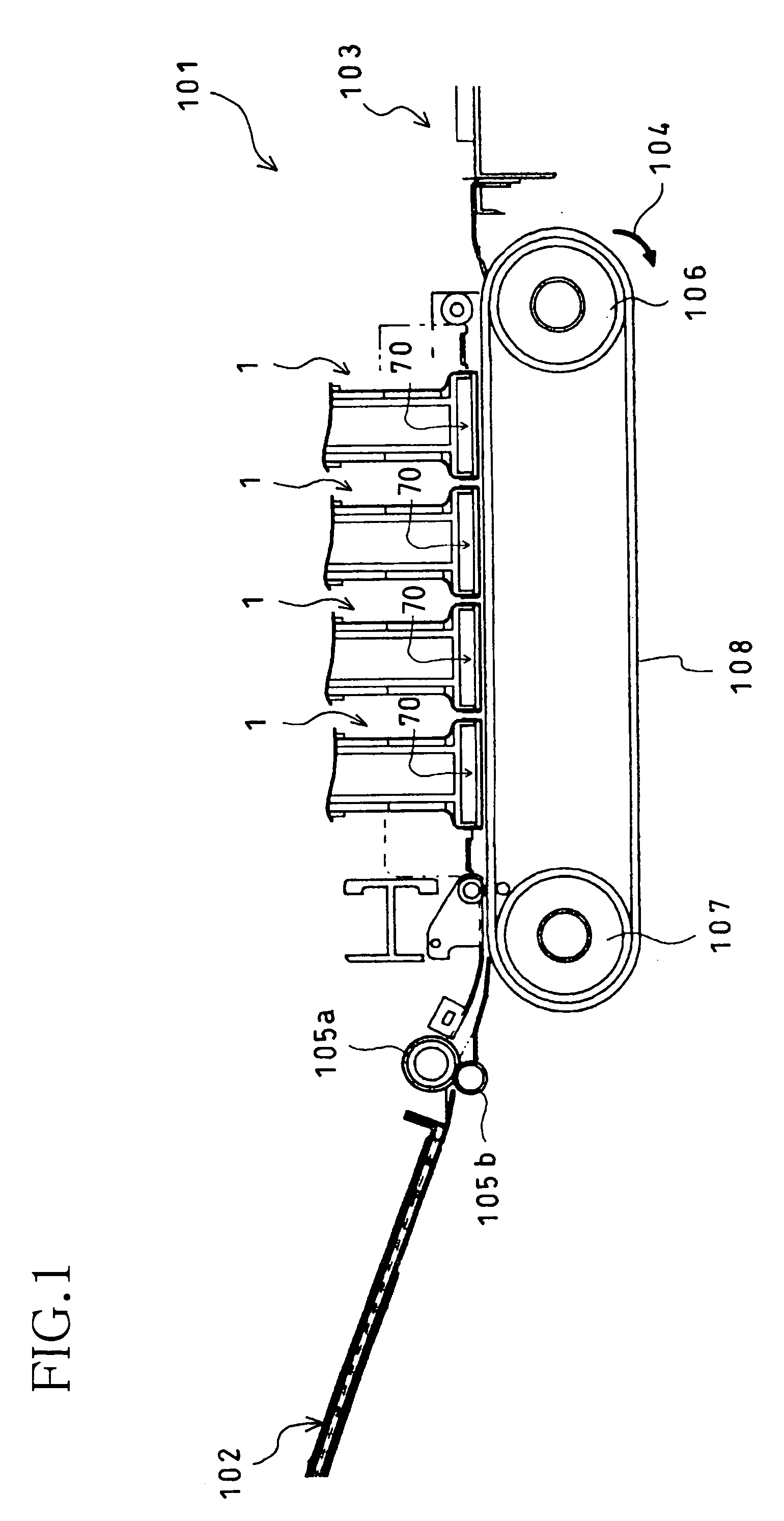
[0041] A general structure of an inkjet printer 101, including a printed circuit board, according to an exemplary embodiment will be described with reference to FIG. 1. The ink-jet printer 101 is a color inkjet printer having four inkjet print heads 1. The printer 101 is provided with a sheet supply unit 102 on the left of FIG. 1 and a sheet discharge unit 103 on the right.

[0042] Inside the printer 101, a sheet feeding path is formed from the sheet supply unit 102 toward the sheet discharge unit 103. Disposed downstream of the sheet supply unit 102 are a pair of feed rollers 105a, 105b that feed a sheet of a recording medium, while holding the sheet between the feed rollers 105a, 105b. The sheet is conveyed by the pair of feed rollers 105a, 105b in a sheet feeding direction from left to right in FIG. 1. Disposed in the middle of the sheet feeding path are two belt rollers 106, 107, a conveyor belt 108, which is endless and looped around the two belt rollers 106, 107, and a conveyor...


PUM

PropertyMeasurementUnit
Electrical conductoraaaaaaaaaa
Areaaaaaaaaaaa

Abstract

A tape substrate includes IC lands electrically connected to pins of a driver IC (integrated circuit), circuit board terminal lands electrically connected to an external circuit board, test lands for testing the driver IC mounted on the tape substrate, and a plating terminal used for plating the land. The test lands are arranged in a matrix. The plating terminal is disposed so as to surround the IC lands, the circuit board terminal lands, and the test lands.

Description

[0001] This application claims priority from JP 2003-423342, filed Dec. 19, 2003, the entire disclosure of which is incorporated herein by reference thereto. BACKGROUND OF THE INVENTION [0002] 1. Field of Invention [0003] This application relates to a method for manufacturing a printed circuit board that mounts an integrated circuit device thereon, and to the printed circuit board. [0004] 2. Description of Related Art [0005] Semiconductor devices are becoming smaller in size, due to demands to downsize electronic apparatuses. Accordingly, pins for inputting or outputting an electric signal to or from the semiconductor devices are getting miniaturized and provided at a narrow pitch. As a semiconductor device is further miniaturized with its pins provided at a narrower pitch, a probe of a tester will accidentally contact pins other than a particular pin of the semiconductor device mounted on a printed circuit board when the device is tested. Therefore, test lands that are respectively...

Claims


Application Information

Patent Timeline
IPC IPC(8): H01L23/498H05K1/00H05K3/34H05K1/02H05K3/24H05K3/28
CPCH01L23/4985Y10T29/49147H05K1/0393H05K3/242H05K3/243H05K3/28H05K2201/0397H05K2203/0191H05K2203/1545H05K2203/175H01L2924/0002H05K1/0268Y10T29/49155Y10T29/49204Y10T29/49169Y10T29/4913H01L2924/00
Inventor ITO, KOJI
Owner BROTHER KOGYO KK
Why Eureka
Try Eureka