

Semiconductor memory device having self-aligned charge trapping layer and method of manufacturing the same
a memory device and self-aligning technology, applied in the direction of semiconductor devices, electrical appliances, transistors, etc., can solve the problems of high initial threshold voltage, high programming current, and high electrical power dissipation of devices, so as to avoid problems such as the problem of conventional local sonos nonvolatile memory devices
- Summary
- Abstract
- Description
- Claims
- Application Information
AI Technical Summary
Benefits of technology
Problems solved by technology
Method used
Image

Examples
Embodiment Construction
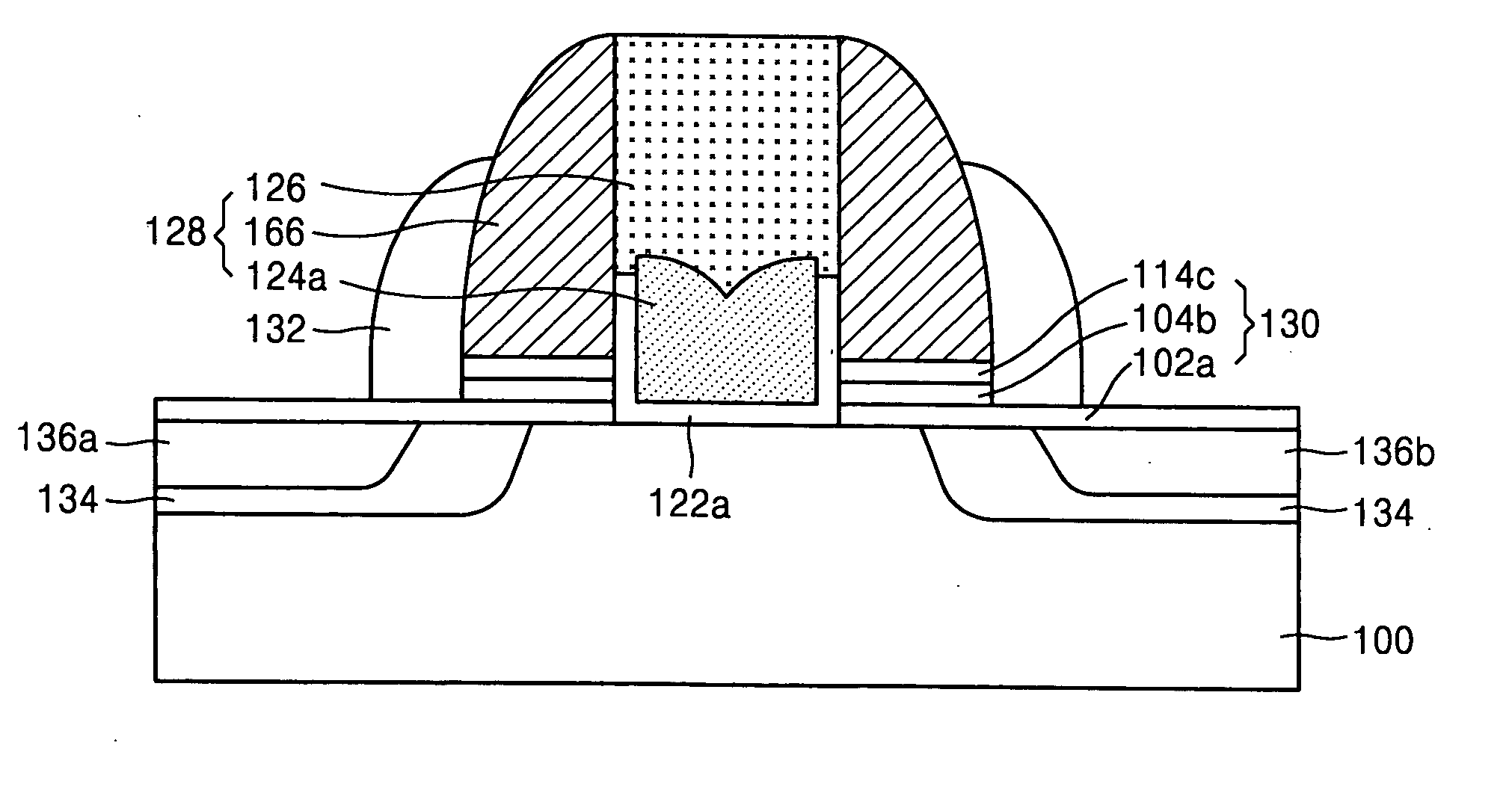
[0036] The length of a charge trapping layer in a semiconductor memory device according to the present invention is determined in one aspect by self-alignment using a conductive spacer. By doing so, the length of the charge trapping layer is defined without the use of a plurality of photolithography processes. As a result, length variations in the charge trapping layer caused by photolithography misalignments are prevented. The present invention will be described in conjunction with a 2-bit cell structure, in which a single gate includes two charge trapping layers. However, this is just a selected teaching example. The present invention is not limited to a 2-bit cell structure.
[0037]FIG. 6 is a sectional view showing a semiconductor memory device including a self-aligned charge trapping layer according to one presently preferred embodiment of the invention.
[0038] Referring to FIG. 6, the memory device includes semiconductor substrate 100 having source and drain regions 136a and 13...
PUM
 Abstract
Description
Claims
Application Information