Vertical gate semiconductor device and method for fabricating the same

Active Publication Date: 2005-06-23
PANASONIC SEMICON SOLUTIONS CO LTD
View PDF5 Cites 29 Cited by
  • Summary
  • Abstract
  • Description
  • Claims
  • Application Information

AI Technical Summary

Benefits of technology

[0024] The present invention has been made in view of the above problems and has its object of providing a vertical gate semicond

Problems solved by technology

However, such a smaller contact area between the common electrode and the body contact region leads

Method used


Image

  • Vertical gate semiconductor device and method for fabricating the same
  • Vertical gate semiconductor device and method for fabricating the same
  • Vertical gate semiconductor device and method for fabricating the same

Examples


first embodiment

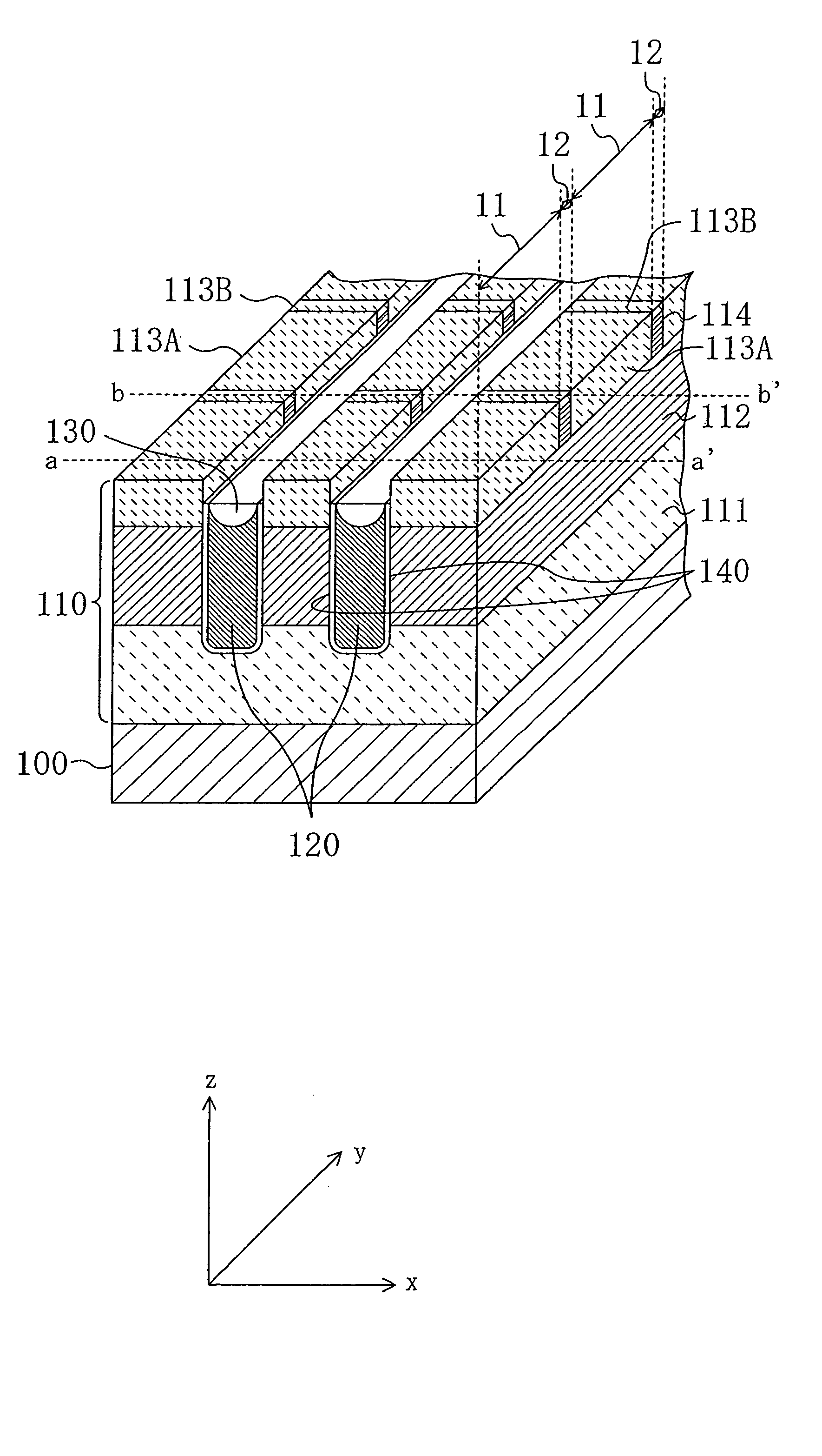
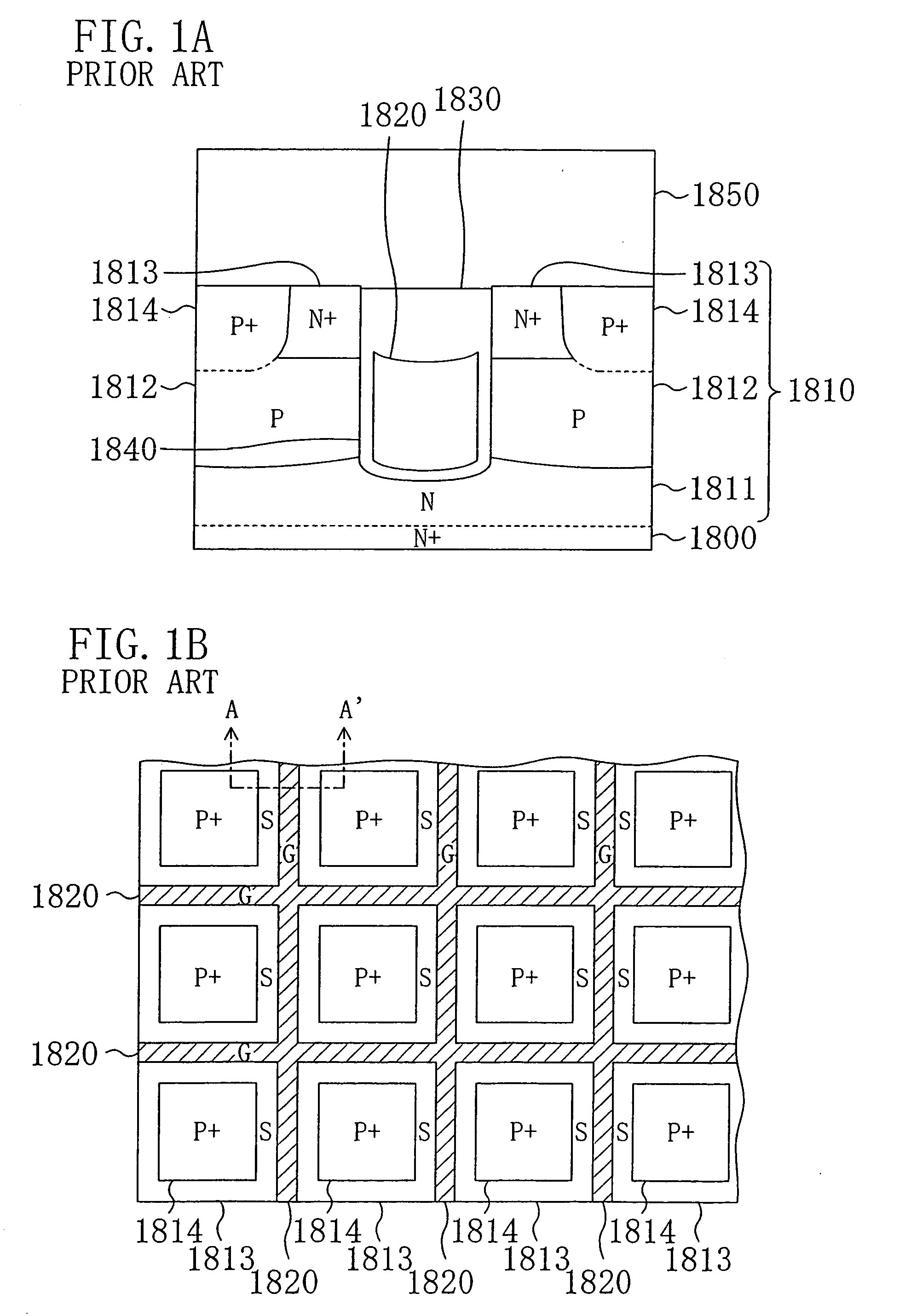
[0081] A vertical gate semiconductor device according to the first embodiment of the present invention will be described below with reference to accompanying drawing. It is noted that the vertical gate semiconductor device in the present embodiment is intended to compact the device without increase in contact resistance of the source region invited.

[0082]FIG. 3 is a bird's eye view (3-dimentional view) of the vertical gate semiconductor device of the present embodiment. As shown in FIG. 3, in the vertical gate semiconductor device of the present embodiment, a semiconductor layer 110 is formed on a N+-type silicon substrate 100 serving as a first conductivity type semiconductor substrate by for example, an epitaxial growth method. A plurality of trenches extending in stripes in the aforementioned semiconductor layer 110 are formed and a vertical gate electrode 120 is buried in each of the trenches. Also, a buried insulating film 130 is formed on the vertical gate electrode 120 in ea...

second embodiment

[0122] A vertical gate semiconductor device and a method of fabricating it according to the second embodiment of the present invention will be described below with reference to the drawings. It is noted that the vertical gate semiconductor device in the present embodiment is intended to compact the device without increase in contact resistance of the source region invited, similar to the first embodiment.

[0123] The difference of the present embodiment from the first embodiment is that a region (corresponding to the body contact region 114 in the first embodiment) having a relatively high impurity concentration (e.g., 5×10¹⁹ to 1×10²⁰ count / cm3) is not formed in the upper portion of the body region 112 having a relatively low impurity concentration (e.g., in the order of 1017 count / cm3) in the second region 12 (see FIG. 11B and FIG. 13B). Wherein, the body region 112 of the second region 12 in the present embodiment has an impurity concentration (e.g., in the order of 1018 count / cm3...


PUM


Abstract

A first region 11 functioning as a transistor includes a drain region 111, a body region 112 formed over the drain region 111, a source region 113A formed over the body region 112 and a trench formed through the body region 112 and having a gate electrode 120 buried therein. A source region 113B is formed over the body region 112 extending in a second region 12.

Description

[0001] This is a continuation of Application PCT / JP2004 / 008363, filed Jun. 8, 2004, now abandoned.FIELD OF THE INVENTION [0002] The present invention relates to semiconductor devices having vertical gate electrodes and methods for fabricating the same. BACKGROUND ART [0003] In association with lowering in power consumption and increase in functionality and in speed of electronics equipment, lower power consumption or higher speed operation is demanded in semiconductor devices accompanied by such equipment. In order to satisfy such demands, low ON resistance of transistors is required in semiconductor devices generally used in DC-DC converters of electronics equipment. As one method for reducing the ON resistance of transistors, the density of the transistors arranged per unit area may be increased. [0004] Specifically, a method has been proposed in which a gate electrode of a semiconductor device is arranged vertically (along a direction perpendicular to the principal plane of the s...

Claims


Application Information

Patent Timeline
IPC IPC(8): H01L21/331H01L21/336H01L21/8234H01L29/06H01L29/08H01L29/10H01L29/417H01L29/739H01L29/78
CPCH01L21/823487H01L29/0696H01L29/0865H01L29/7813H01L29/41766H01L29/7808H01L29/1095H01L29/66734
Inventor MIZOKUCHI, SHUJIYAMANAKA, MITSUHIROGUNJI, HIROYUKI
Owner PANASONIC SEMICON SOLUTIONS CO LTD
Why Eureka
Try Eureka