
Data strobe circuit using clock signal

Active Publication Date: 2005-06-23
SK HYNIX INC
View PDF8 Cites 5 Cited by
  • Summary
  • Abstract
  • Description
  • Claims
  • Application Information

AI Technical Summary

Benefits of technology

[0010] Accordingly, it is an object of the present invention to provide a data strobe circuit for generating an internal strobe signal for latching data in a test mode not by externally applied data latch input signals such as LDQS, LDQSB and VREF but by a reference clock signal CLK of a memory device, thereby reducing the number of pins required to test each memory device to measure a larger number of chips simultaneously.

Problems solved by technology

Recently, the main issue of the semiconductor memory field has been in a transition from integration to the operation speed.
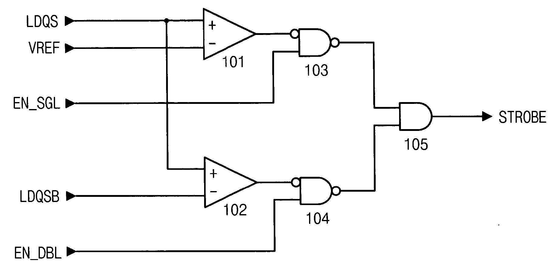
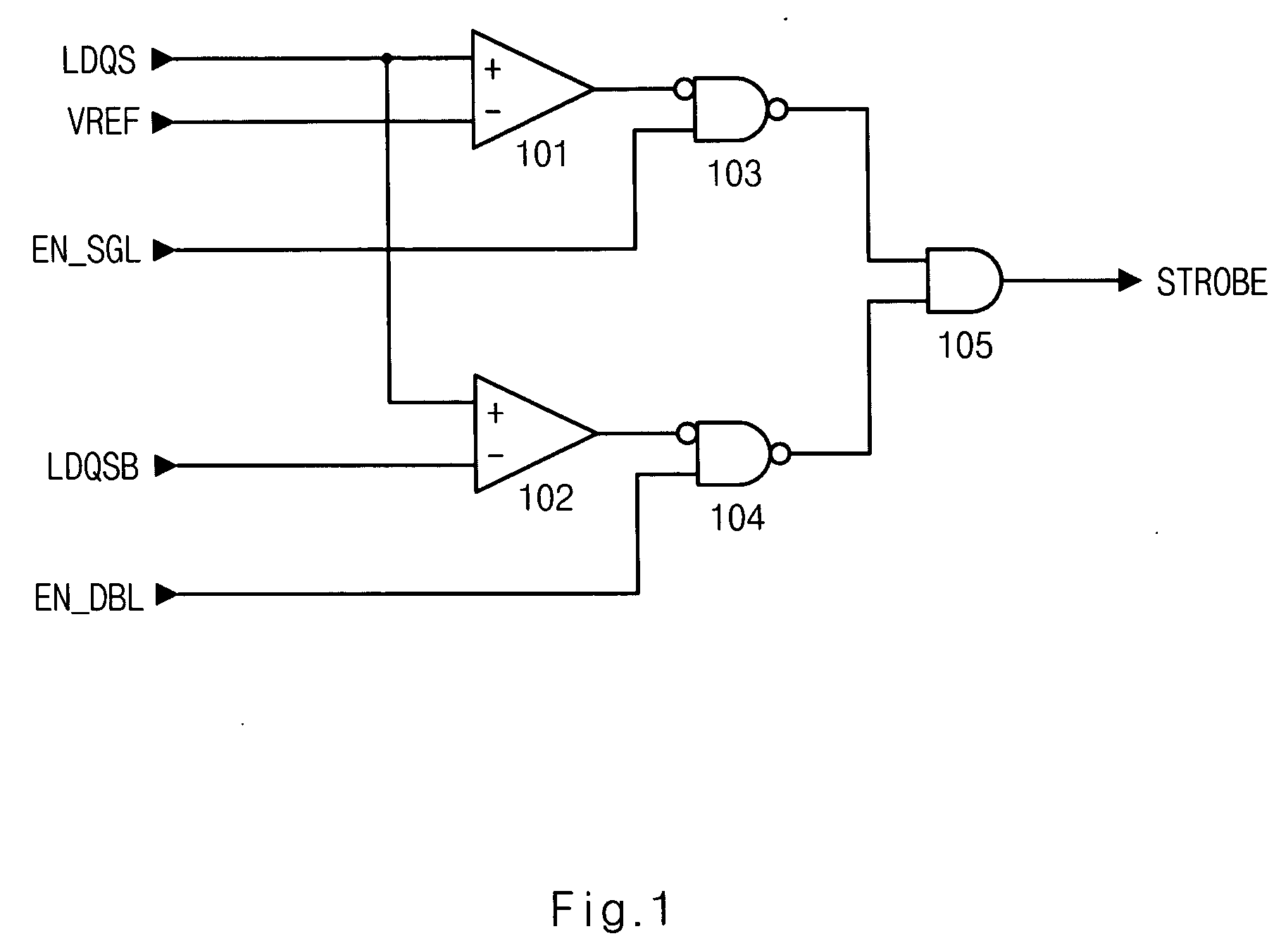
As a result, the large amount of chips cannot be tested at the same time due to the restriction of the number of pins in the conventional memory device which requires external input signals such as the data strobe signals LDQS and LDQSB and the reference voltage VREF to generate the internal strobe signal STROBE.

Method used


Image

  • Data strobe circuit using clock signal
  • Data strobe circuit using clock signal
  • Data strobe circuit using clock signal

Examples


first embodiment

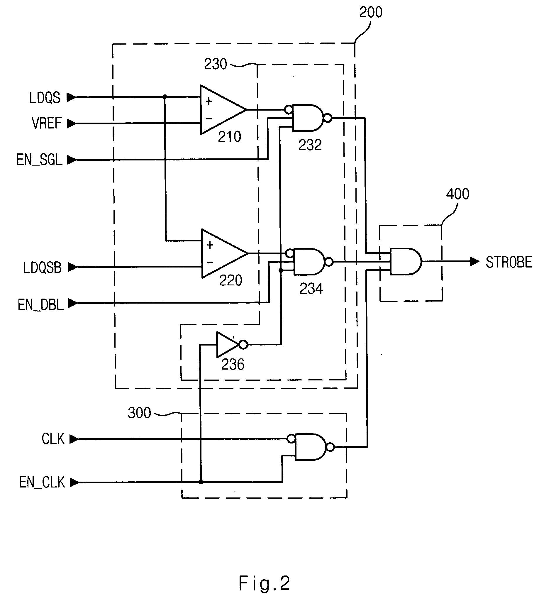
[0018]FIG. 2 is a circuit diagram illustrating a data strobe circuit using a clock signal according to the present invention.

[0019] In an embodiment, the data strobe circuit comprises an external input processing unit 200, a clock signal processing unit 300 and a strobe signal output unit 400.

[0020] The external input processing unit 200 performs a logic operation on data strobe signals LDQS and LDQSB applied externally and a reference voltage VREF, and selectively outputs the result of the logic operation in response to internal control signals EN_SGL and EN_DBL and a clock enable signal EN_CLK. The external input processing unit 200 comprises a first comparison unit 210, a second comparison unit 220 and a selective output unit 230. Here, the clock enable signal EN_CLK which controls generation of the internal strobe signal STROBE in response to a clock signal CLK in a test mode is activated in the test mode and inactivated in a normal mode.

[0021] The first comparison unit 210 co...

second embodiment

[0034]FIG. 3 is a circuit diagram illustrating a data strobe circuit using a clock signal according to the present invention.

[0035] The data strobe circuit of FIG. 3 comprises an external input processing unit 500 and a clock signal processing unit 600.

[0036] The external input processing unit 500 performs a logic operation on data strobe signals LDQS and LDQSB applied externally and a reference voltage VREF, and outputs the result of the logic operation as an internal strobe signal STROBE in response to internal control signals EN_SGL and EN_DBL when a clock enable signal EN_CLK is inactivated. Here, the external input processing unit 500 comprises a third comparison unit 510, a fourth comparison unit 520 and a selective output unit 530.

[0037] The third comparison unit 510 compares the data strobe signal LDQS with the reference voltage VREF, and outputs the result of the comparison. Here, the third comparison unit 510 comprises a comparator for comparing the level of the data str...


PUM


Abstract

A data strobe circuit is configured to generate an internal strobe signal for latching data in response to a clock signal. The data strobe circuit using a clock signal comprises an external input processing unit, a clock signal processing unit and a strobe signal output unit. The external input processing unit performs a logic operation on an externally applied data strobe signal and a reference voltage, and outputs the result of the logic operation in response to a clock enable signal and an internal control signal. The clock signal processing unit selectively outputs an external clock signal in response to the clock enable signal. The strobe signal output unit performs a logic operation on output signals from the external input processing unit and the clock signal processing unit, and selectively outputs one of the output signals from the external input processing unit and the clock signal processing unit as an internal data strobe signal.

Description

BACKGROUND OF THE INVENTION [0001] 1. Field of the Invention [0002] The present invention generally relates to a data strobe circuit, and more specifically, to an improved data strobe circuit for generating an internal strobe signal not by a data strobe signal applied externally but by a clock signal in a wafer test, thereby testing the larger number of chips at a wafer state simultaneously. [0003] 2. Description of the Prior Art [0004] Recently, the main issue of the semiconductor memory field has been in a transition from integration to the operation speed. As a result, high speed synchronous memories such as a DDR SDRAM (Double Data Rate Synchronous DRAM) and a RAMBUS DRAM has been focused as a new issue in the semiconductor memory field. [0005] The synchronous memory which refers to a memory operated synchronously with respect to an external system clock includes a SDRAM which leads the current mass production memory market of DRAMs. The SDRAM performs once data access at every ...

Claims


Application Information

Patent Timeline
IPC IPC(8): G11C5/00G11C11/40G11C8/18G11C29/00G11C29/14
CPCG11C29/006G11C29/14G11C29/12015G11C11/40
Inventor LEE, KANG YOUL
Owner SK HYNIX INC
Learn More