Semiconductor light emitting element and fabrication method thereof

a technology of semiconductors and light emitting elements, applied in semiconductor lasers, lasers, solid-state devices, etc., can solve the problems of difficult dispersion, low light extraction efficiency, and difficult workability and repeatability, and achieve good workability and repeatability, and high light extraction efficiency

Inactive Publication Date: 2005-06-30
SANKEN ELECTRIC CO LTD
View PDF3 Cites 15 Cited by
  • Summary
  • Abstract
  • Description
  • Claims
  • Application Information

AI Technical Summary

Benefits of technology

[0013] In view of the above-described circumstance, it is an object of the present invention to provide a semiconductor light emitting element which has a high light extraction efficiency and can be fabricated with a good workability and repeatability, and a fabrication method thereof.

Problems solved by technology

Since the difference in the refraction index between the surface layer and the outside world is relatively large, the light extraction efficiency is relatively low.
However, the formation of such a scattering layer has problems in the viewpoints of workability and repeatability.
However, it is extremely difficult to carry out the dispersion with a good repeatability and fabricate light emitting elements having a high uniformity and a desired luminance at a high yield.
However, this method also has the workability problem, and formation of recesses and bosses might give an adverse influence on the electric property of the light emitting element.

Method used


Image

  • Semiconductor light emitting element and fabrication method thereof
  • Semiconductor light emitting element and fabrication method thereof
  • Semiconductor light emitting element and fabrication method thereof

Examples


Embodiment Construction

[0062] A semiconductor light emitting element according to the embodiment of the present invention will now be specifically explained with reference to the drawings. The following will explain, as an example, a case where a semiconductor light emitting element forms a light emitting diode.

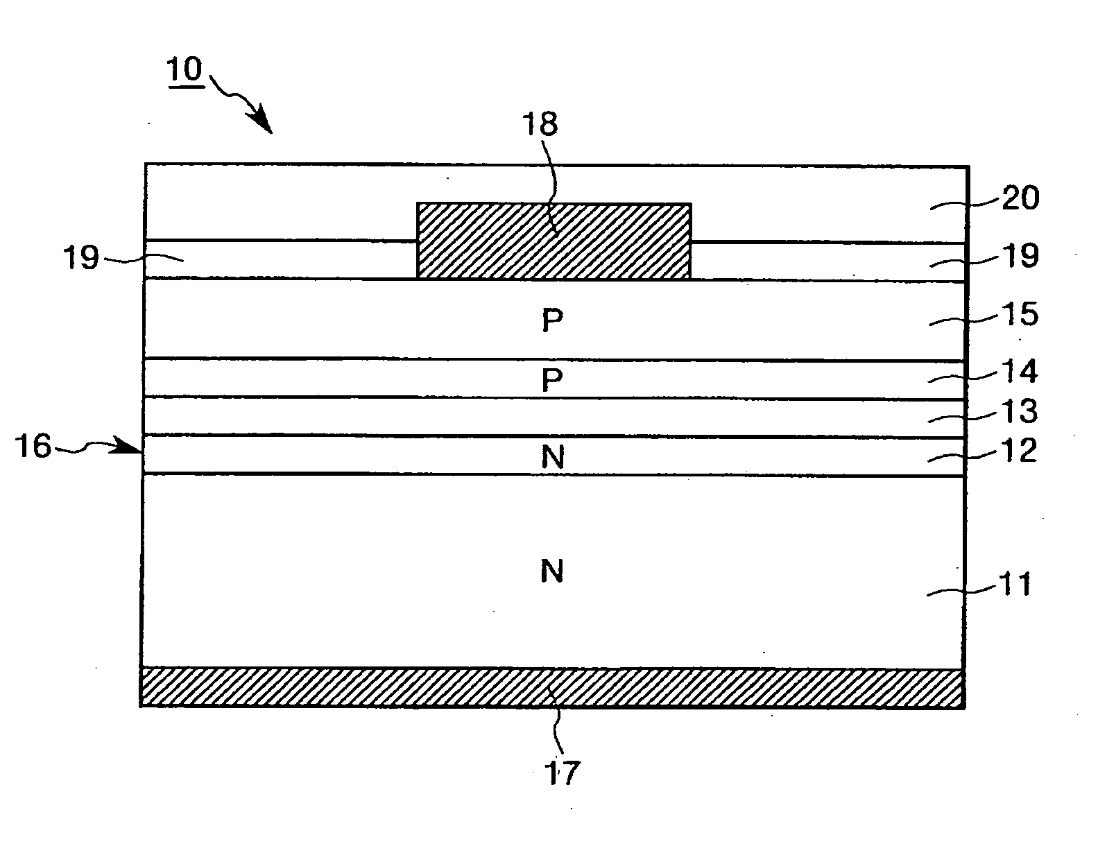
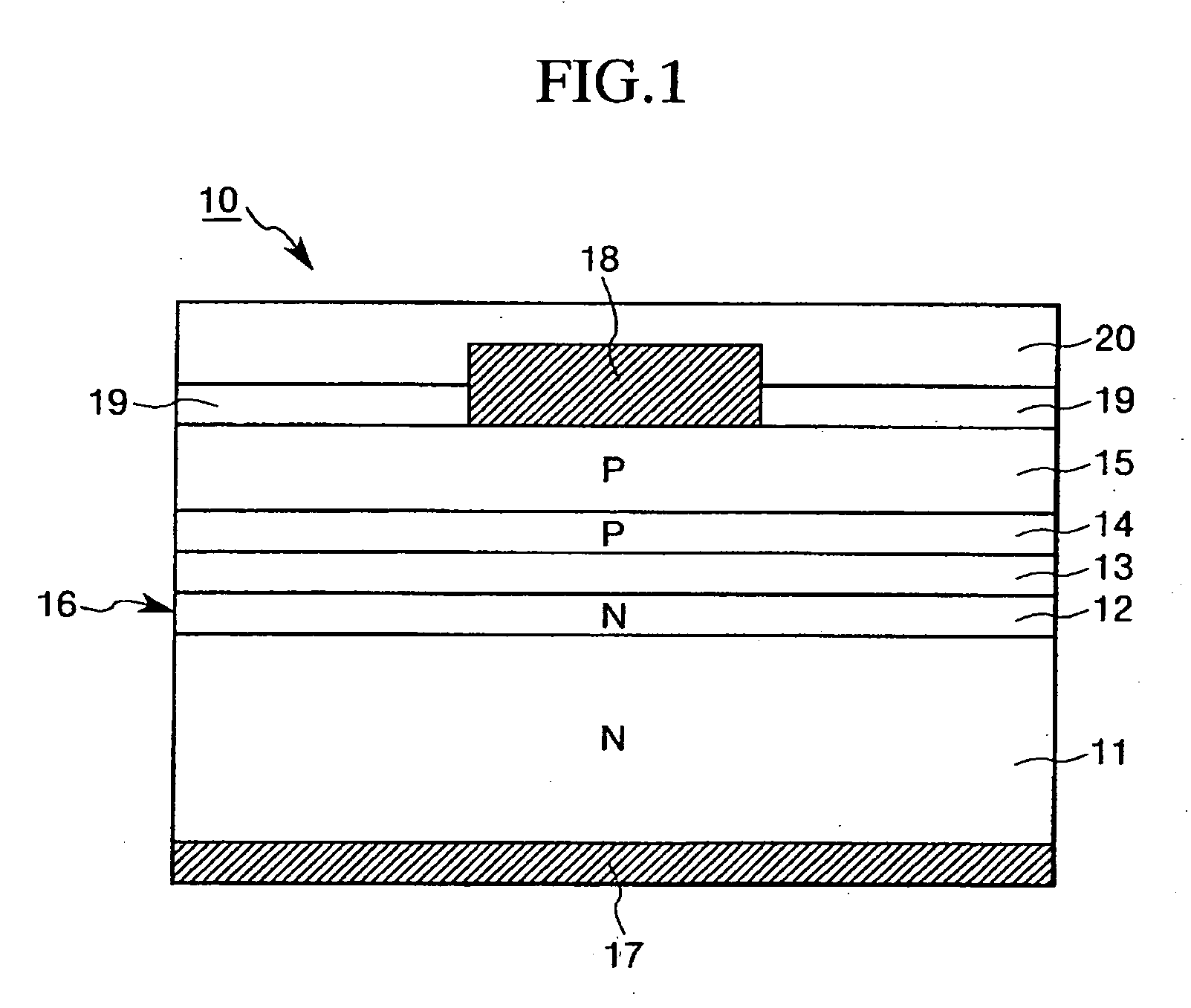
[0063]FIG. 1 shows a cross-sectional view of a semiconductor light emitting element 10 according to the embodiment of the present invention. As shown in FIG. 1, the semiconductor light emitting element 10 according to the present embodiment comprises a semiconductor base 16 including an N-type substrate 11, an N-type auxiliary layer 12, an active layer 13, a P-type auxiliary layer 14, and a window layer 15. The semiconductor light emitting element 10 is formed of a cathode electrode 17 which is formed on one surface of the semiconductor base 16, and of an anode electrode 18, a light transmissive layer 19, and a protection layer 20 which are formed on the other surface thereof.

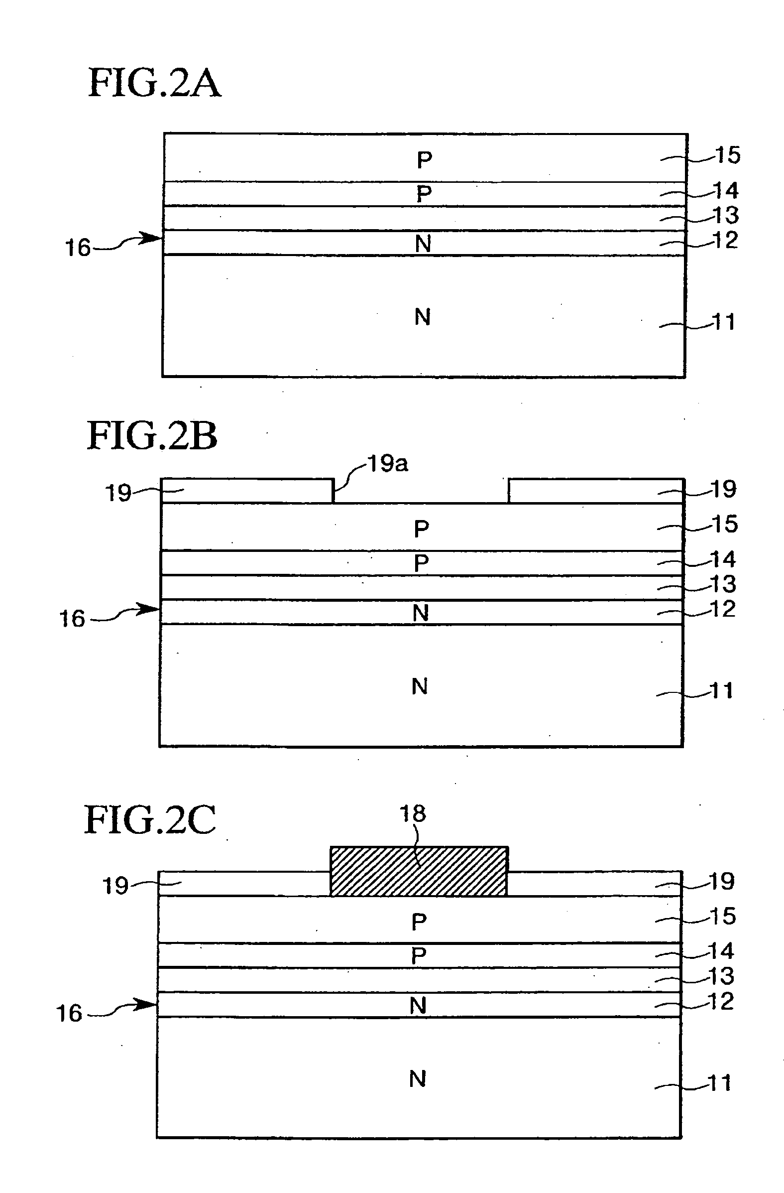
[0064] As shown in F...


PUM


Abstract

Provided between a window layer and a protection layer is a light transmissive layer having a refraction index which is between the refraction indexes of the window layer and protection layer. The refraction index n2 of the light transmissive layer is, for example, within ±20% of the geometric average of the refraction indexes of the window layer and protection layer. The thickness T of the light transmissive layer satisfies {(λ/4n2)×(2m+1)−(λ/8n2)≦T≦(λ/4n2)×(2m+1)+(λ/8n2)} where λ represents the wavelength of emitted light and m represents a positive integer not smaller than 0.

Description

CROSS-REFERENCES TO RELATED APPLICATIONS [0001] This application is based on Japanese Patent Application No. 2003-429716 filed on Dec. 25, 2003, the disclosure of which is incorporated herein by reference in its entirety. BACKGROUND OF THE INVENTION [0002] 1. Field of the Invention [0003] The present invention relates to a semiconductor light emitting element such as a light emitting diode, a semiconductor laser, etc. and a fabrication method thereof. [0004] 2. Description of the Related Art [0005] To improve the luminance of a semiconductor light emitting element such as a light emitting diode, a semiconductor laser, etc., it is extremely important to efficiently extract the light emitted in the active layer of the light emitting element to the outside of the element. That is, it is necessary to restrict light reflection on the surface of the light emitting element as much as possible to let out the emitted light to the outside of the element and increase the so-called light extrac...

Claims


Application Information

Patent Timeline
Patent Type & Authority Applications(United States)
IPC IPC(8): H01L27/15H01L33/14H01L33/30H01L33/40H01S5/00
CPCH01L33/56H01L33/44
Inventor MUROFUSHI, HITOSHITAKEDA, SHIRO
Owner SANKEN ELECTRIC CO LTD
Why Eureka
Try Eureka