Semiconductor device and fabrication method thereof

Active Publication Date: 2005-06-30
RENESAS ELECTRONICS CORP
View PDF6 Cites 14 Cited by
  • Summary
  • Abstract
  • Description
  • Claims
  • Application Information

AI Technical Summary

Benefits of technology

[0018] According to the present invention, a part of the capacitor-insulator layer is etched in the first etching step in which the second conductive layer is etched, and the remaining part of the capacitor-insulator layer is etched in the second etching step in which the first conductive layer is etched. Thus, an MiM capacitor element can be formed by performing photolithography twice. Therefore, a fabrication cost of the semiconductor device is reduced. Moreover, the first conductive layer is not exposed to the outside in the first etching step. Therefore, no conductive deposit adheres to the side faces of the upper electrode. In addition, in the second etching step, no conductive deposit adheres to the side faces of the upper electrode and the side faces of the capacitor-insulator layer because the second resist pattern covers the side faces of the upper electrode and the side faces of the capacitor-insulator layer. Thus, in the MiM capacitor element, a leak cu

Problems solved by technology

This means that a fabrication cost is expensive.
However, the conven

Method used


Image

  • Semiconductor device and fabrication method thereof
  • Semiconductor device and fabrication method thereof
  • Semiconductor device and fabrication method thereof

Examples


Example

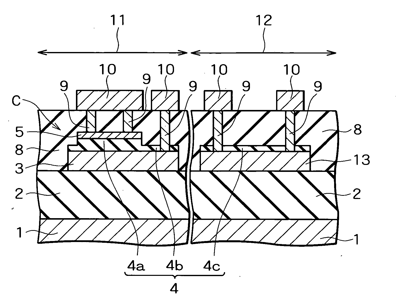
[0031] A preferred embodiment of the present invention will be now described specifically, referring to attached drawings. FIG. 5 is a cross-sectional view of a semiconductor device according to an embodiment of the present invention. The components of the semiconductor device shown in FIG. 5, which are the same as those of the conventional semiconductor device described above, are labeled with the same reference numerals as those in FIGS. 1 to 4.

[0032] As shown in FIG. 5, in the semiconductor device of the present embodiment, an MiM region 11 in which an MiM capacitor element C is formed and a wiring region 12 in which a wiring is formed are provided. Moreover, on a silicon substrate 1 formed of P type silicon, for example, an insulation layer 2 is provided. The insulation layer 2 is formed of silicon oxide, for example, and has a thickness of from 1 to 5 μm, for example.

[0033] In the MiM region 11, a lower electrode 3 is provided on the insulation layer 2. In the wiring region 1...


PUM


Abstract

On a silicon substrate, a first insulation layer, a lower conductive layer, a capacitor-insulator layer, and an upper conductive layer are formed in that order. Then, a first resist pattern is formed, the upper conductive layer is etched to form an upper electrode, and the capacitor-insulator layer is successively etched partway under the same etching condition as that of the upper conductive layer. Next, second resist pattern is formed, the remaining part of the capacitor-insulator layer is etched to form a second insulation layer, and the lower conductive layer is successively etched under the same etching condition as that of the capacitor-insulator layer so as to form a lower electrode and a lower wiring. In this manner, an MiM capacitor element constituted by the upper electrode, a part of the second insulation layer, and the lower electrode can be fabricated.

Description

BACKGROUND OF THE INVENTION [0001] 1. Field of the Invention [0002] The present invention relates to a semiconductor device including an MiM (Metal Insulator Metal) capacitor element and a fabrication method thereof. The present invention can be applied to fabrication of a capacitor element using photolithography. In particular, the present invention is suitable for fabrication of an MiM capacitor element in a semiconductor device. [0003] 2. Description of the Related Art [0004] Conventionally, an MiM capacitor element is used as a capacitor element formed in a semiconductor device. The MiM capacitor element has a lower electrode formed of metal or alloy (hereinafter, collectively referred to as metal), an upper electrode formed of metal, and an insulation layer formed between the lower and upper electrodes. (See Japanese Patent Laid-Open Publication No. 2003-31665, FIGS. 1 to 3, for example.) [0005] A fabrication method of the MiM capacitor element disclosed in Japanese Patent Laid...

Claims


Application Information

Patent Timeline
IPC IPC(8): H01L21/02H01L21/822H01L23/522H01L27/04
CPCH01L28/40H01L23/5223H01L2924/0002H01L2924/00
Inventor OHKUBO, HIROAKIYAMAMOTO, RYOTAFURUMIYA, MASAYUKISATO, MASAHARUKIKUTA, KUNIKONAKAYAMA, MAKOTONAKASHIBA, YASUTAKA
Owner RENESAS ELECTRONICS CORP
Why Eureka
Try Eureka