Method for forming metal wiring in semiconductor device

Inactive Publication Date: 2005-06-30
STMICROELECTRONICS SRL +1
View PDF15 Cites 2 Cited by
  • Summary
  • Abstract
  • Description
  • Claims
  • Application Information

AI Technical Summary

Benefits of technology

[0015] The present invention is directed to a method for forming metal lines in a semiconductor device which can reduce an RC delay time and form highly reliable metal lines, by restricting crosstalk between the metal lines and decreasing

Problems solved by technology

However, the Cu lines are hardly dry-etched and easily corroded in air, and Cu atoms are easily diffused into an insulation film.
As a result, an RC delay time seriously increases due to high crosstalk and capacitance between the Cu lines.
Increase of the RC delay time decreases reliability of the device and prevents high integration of the device.
Such problems result from difficulty of the Cu line process.
Accordingly, a critical value of the interlayer insulation film for insulating the Cu lines is not obtained, and thus an RC delay time increases due to high crosstalk and capacitance between the adjacent Cu lines.
Second, when the damascene patterns are small, Cu cannot be regularly filled without pores by a general physical vapor deposition (PVD) or chemical vapor deposition (CVD).
It is thus

Method used


Image

  • Method for forming metal wiring in semiconductor device
  • Method for forming metal wiring in semiconductor device
  • Method for forming metal wiring in semiconductor device

Examples


Example

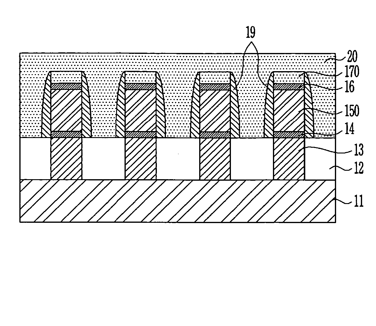
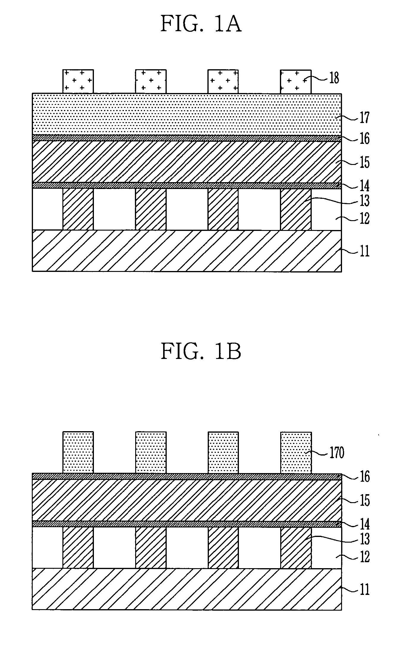
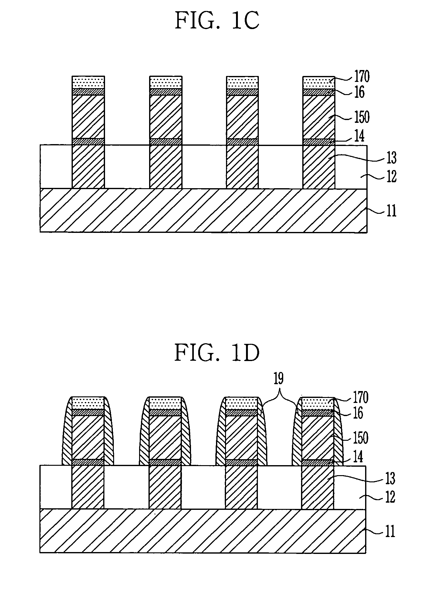
[0021] A method for forming metal lines in a semiconductor device in accordance with a preferred embodiment of the present invention will now be described in detail with reference to the accompanying drawings.

[0022] In case it is described that one film is disposed on or contacts another film or a semiconductor substrate, one film can directly contact another film or the semiconductor substrate, or the third film can be positioned between them. In the drawings, a thickness or size of each layer may be exaggerated to provide easy and clear explanations. Wherever possible, the same reference numerals will be used throughout the drawings and the description to refer to the same or like parts.

[0023]FIGS. 1A to 1E are cross-sectional diagrams illustrating sequential steps of the method for forming the metal lines in the semiconductor device in accordance with the preferred embodiment of the present invention.

[0024] Referring to FIG. 1A, a first interlayer insulation film 12 is formed ...


PUM


Abstract

The present invention discloses a method for forming metal lines in a semiconductor device. A plurality of metal lines are densely formed by using Al or Al alloy as a material and performing a reactive ion etching process using a low-k dielectric layer as hard mask patterns. Barrier metal layers are formed on the sidewalls of the metal lines. A low dielectric interlayer insulation film is formed when the low dielectric hard mask patterns exist. It is thus possible to obtain margins in a line process and gains in a critical value of the interlayer insulation film for insulating the metal lines. Therefore, a RC delay time can be reduced by restricting crosstalk between the metal lines and decreasing a capacitance between the metal lines.

Description

BACKGROUND [0001] 1. Field of the Invention [0002] The present invention relates to a method for forming metal lines in a semiconductor device, and more particularly to, a method for forming metal lines in a semiconductor device which can reduce an RC delay time by restricting crosstalk between the metal lines and decreasing capacitance between the metal lines, by using a low-k dielectric layer and performing a reactive ion etching (RIE) process. [0003] 2. Discussion of Related Art [0004] According to a high integration, high function and miniaturization tendency of a semiconductor device, a material which is advantageous in an RC delay time due to a low specific resistance, and which is highly resistible to electromigration (EM) and stressmigration (SM) is required as a material of metal lines. Instead of Al which has been generally used as the most appropriate material of the metal lines, Cu newly attracts attention. [0005] Cu is used as the material of the metal lines because a m...

Claims


Application Information

Patent Timeline
IPC IPC(8): H01L21/28H01L21/322H01L21/44H01L21/4763H01L21/768H01L23/522H01L23/532
CPCH01L21/76834H01L21/76852H01L21/7685H01L21/28
Inventor RYU, HYUN KYU
Owner STMICROELECTRONICS SRL
Why Eureka
Try Eureka