Method of manufacturing multilayer wiring substrate, and multilayer wiring substrate

Inactive Publication Date: 2005-06-30
SONY CORP
View PDF13 Cites 10 Cited by
  • Summary
  • Abstract
  • Description
  • Claims
  • Application Information

AI Technical Summary

Benefits of technology

[0025] According to the present invention, the second wiring substrate can be formed smaller in area than the first wiring substrate. Thus, as compared with the case in which the second wiring substrate is formed on the entire surf

Problems solved by technology

In association with the miniaturization and the usage of multiple functions in electronic apparatuses, the request for higher density of wiring substrates (printed circuit boards) and miniaturization of mounted parts are becoming increasingly restrictive.
Thus, this method has a problem that the expansion/contraction and the warp of the transfer sheet 7 occurring at a time of handling cause an error to be easily induced in the pattern shapes (the dimensions) of the transferred conductor patterns 6, 11.
Thus, in this conventional method of manufacturing the multilayer wiring substrate, it will be very difficult to cope with the hyperfine structure (fine pitch structure) of the conductor patterns expected to continue to evolve in the future.
Hence, it is impossible to obtain the multilayer wiring substrate of a high quality which corresponds to the fine pitch structure.
However, in this case, if the rigid property of the tr

Method used


Image

  • Method of manufacturing multilayer wiring substrate, and multilayer wiring substrate
  • Method of manufacturing multilayer wiring substrate, and multilayer wiring substrate
  • Method of manufacturing multilayer wiring substrate, and multilayer wiring substrate

Examples


Example

First Embodiment

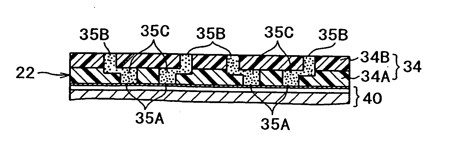
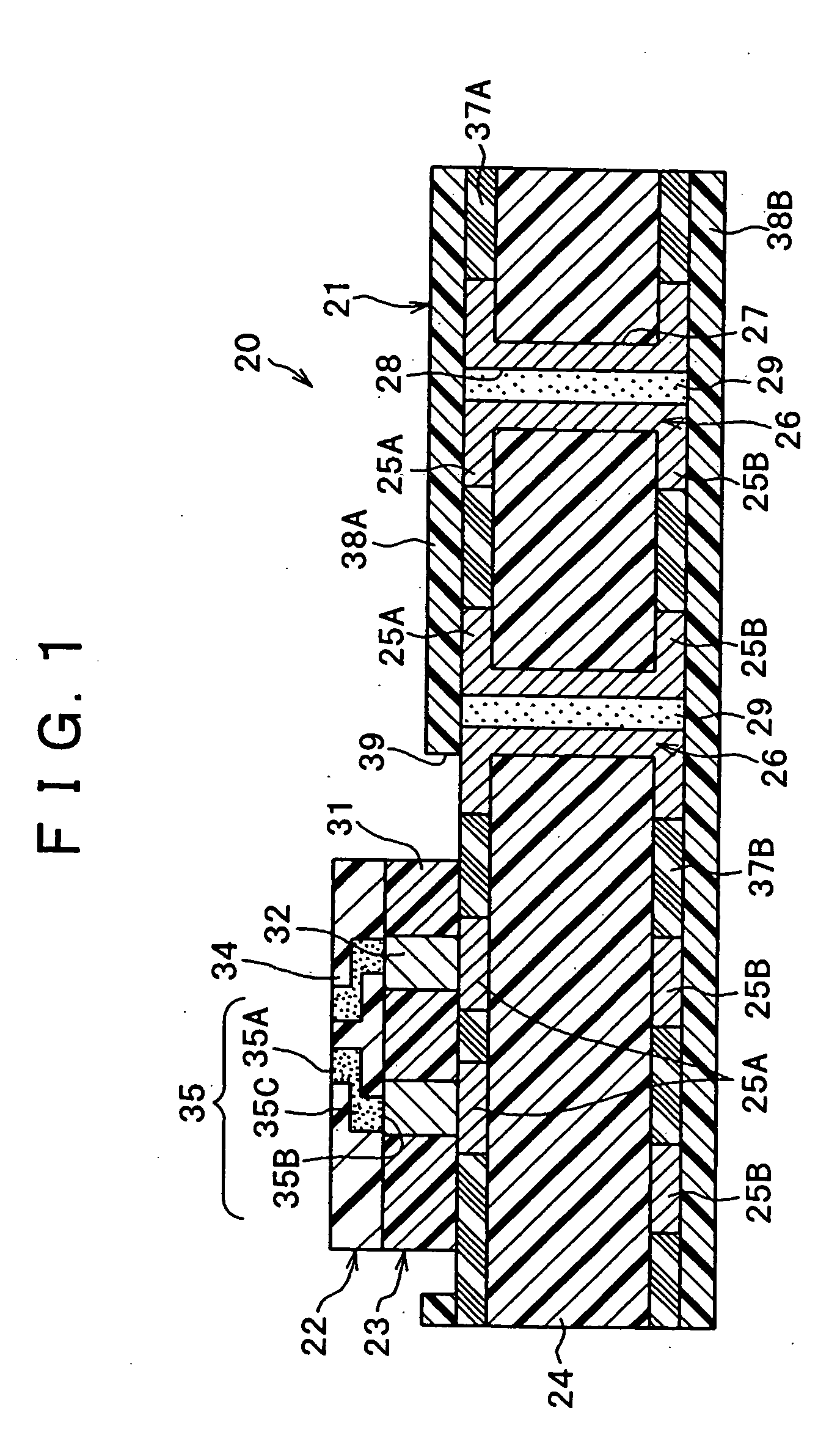
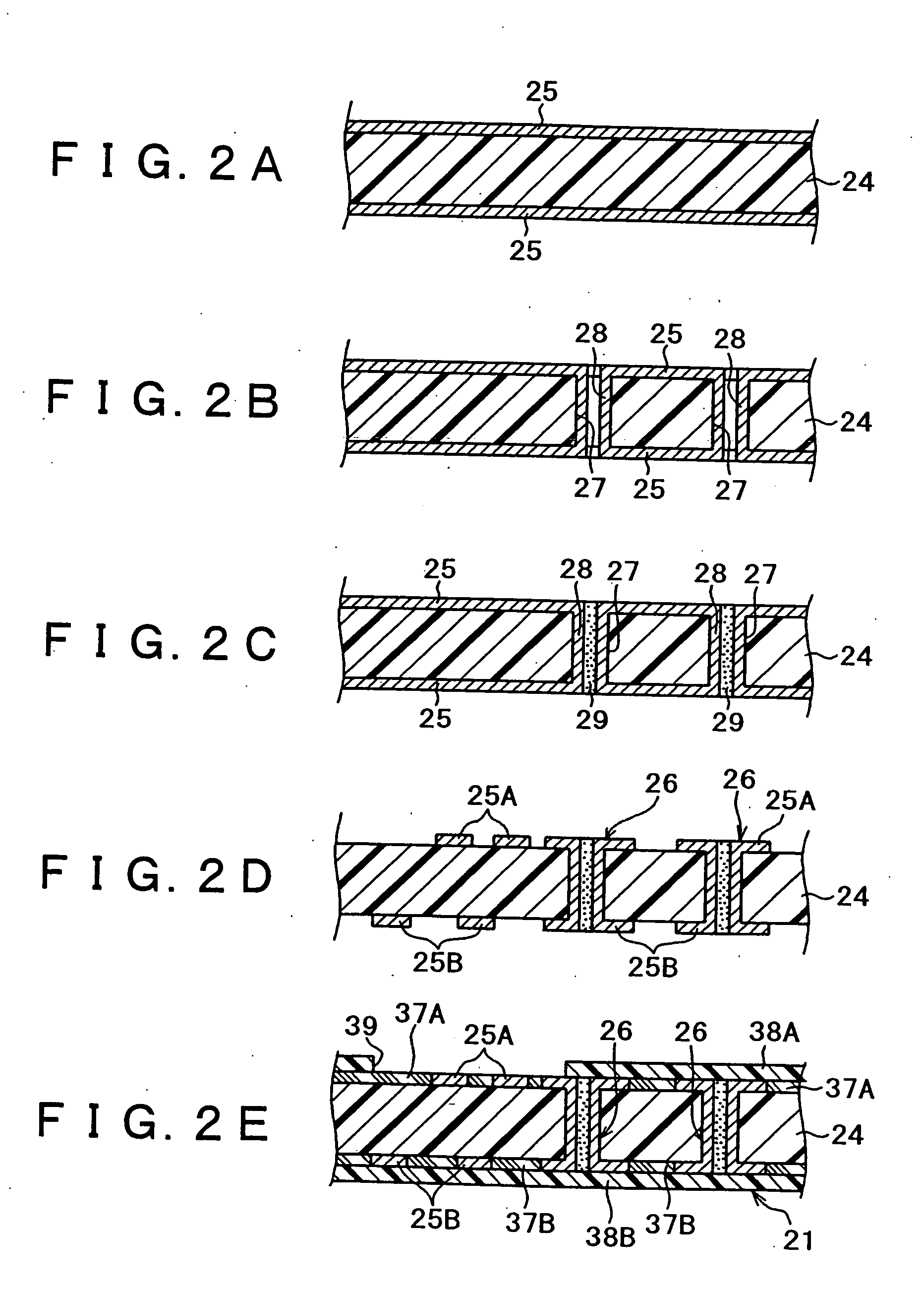
[0057]FIG. 1 shows a configuration of a multilayer wiring substrate according to the first embodiment of the present invention. A multilayer wiring substrate 20 in this embodiment is provided with a first wiring substrate 21, a second wiring substrate 22, and an adhesive material layer 23 placed between those first and second wiring substrates 21, 22.

[0058] The first wiring substrate 21 in this embodiment is made of, for example, double-side copper-clad stack, and it includes: an insulator base material 24 serving as an insulating layer; and conductor patterns 25A, 25B (corresponds to a first conductor pattern of the present invention) formed by patterning copper foils on the double sides to predetermined shapes. By the way, Ni / Au (Nickel / Gold) plating layers may be formed on surface layers of the conductor patterns 25A, 25B.

[0059] The construction material of the insulator base material 24 is suitably selected depending on an application target, a use application...

Example

Second Embodiment

[0103]FIG. 8 shows the configuration of a multilayer wiring substrate according to a second embodiment of the present invention. A multilayer wiring substrate 50 in this embodiment is provided with a first wiring substrate 51, a second wiring substrate 52 and an adhesive material layer 53 placed between those first and second wiring substrates 51, 52.

[0104] The first wiring substrate 51 in this embodiment has the configuration similar to that of the first wiring substrate 21 explained in the first embodiment. It is made of the double-side copper-clad stack, and it includes: an insulator 54 serving as an insulating layer; and conductor patterns 55A, 55B (corresponds to a first conductor pattern of the present invention) formed by patterning the copper foils on the double sides to the predetermined shapes. By the way, the Ni / Au plating layers may be formed on the surface layers of the conductor patterns 55A, 55B.

[0105] The construction material of the insulator 54 ...


PUM

PropertyMeasurementUnit
Shapeaaaaaaaaaa
Electrical conductoraaaaaaaaaa
Photosensitivityaaaaaaaaaa

Abstract

The present invention provides a method of manufacturing a multilayer wiring substrate, which can preserve the dimensional stability of a conductor pattern at a fine pitch, solve the restriction on a process from the viewpoint of material selection, and further reduce a manufacturing cost, and a multilayer wiring substrate. A second wiring substrate formed on a supporting sheet made of metal and an adhesive layer are partially stacked on a predetermined region of a first wiring substrate by using the supporting sheet. After the lamination of the second wiring substrate, the supporting sheet is finally etched and removed. The second wiring substrate is stacked only on the portion required to be multilayered on the first wiring substrate to thereby reduce the amount of the construction material of the second wiring substrate.

Description

BACKGROUND OF THE INVENTION [0001] 1. Field of the Invention [0002] The present invention relates to a method of manufacturing a multilayer wiring substrate in which two or more wiring substrates are stacked on each other, and a multilayer wiring substrate. [0003] 2. Description of Related Art [0004] In association with the miniaturization and the usage of multiple functions in electronic apparatuses, the request for higher density of wiring substrates (printed circuit boards) and miniaturization of mounted parts are becoming increasingly restrictive. In the wiring substrate, the higher density in a direction parallel to a substrate surface has been conventionally tried by reducing a wiring rule. However, in recent years, the higher density in a direction vertical to the surface of the wiring substrate has been advanced by employing a buildup process, stacking the wiring substrates, and forming via holes (interlayer connections) to electrically connect any layers to each other. [000...

Claims


Application Information

Patent Timeline
IPC IPC(8): H05K3/22H01L23/12H05K3/00H05K3/20H05K3/46
CPCH01L21/4846Y10T29/4913H01L23/49833H01L2924/09701H05K3/0023H05K3/205H05K3/4617H05K3/4623H05K3/4694H05K2201/0195H05K2201/09536H05K2201/09881H05K2201/09972H01L2924/0002H01L21/4857Y10T29/49126Y10T29/49128Y10T29/49155Y10T29/49165Y10T29/49124H01L2924/00
Inventor ASAMI, HIROSHIKUSANO, HIDETOSHINISHITANI, YUJIORUI, KEN
Owner SONY CORP
Why Eureka
Try Eureka