Structures and methods for making strained mosfets

a technology of mosfets and finfets, applied in the direction of semiconductor devices, electrical apparatus, transistors, etc., can solve the problems of increasing parasitic junction capacitance, and reducing the size of the devi

Active Publication Date: 2005-07-07
GLOBALFOUNDRIES US INC
View PDF98 Cites 218 Cited by
  • Summary
  • Abstract
  • Description
  • Claims
  • Application Information

AI Technical Summary

Problems solved by technology

As semiconductor devices shrink, traditional device fabrication techniques have approached practical limits in size scaling.
Unwanted short channel effects may be reduced by higher doping concentrations, which lead to the unwanted effects of carrier mobility degradation, increased parasitic junction capacitance, and increased sub-threshold swing if doping concentrations become too high.
However, carefully controlling implantation and annealing adds costs to the fabrication process, and are ultimately limited in effectiveness as channel lengths are further reduced.
Scaling limits imposed due to the limitation of gate oxide thickness and source/drain junction depth

Method used


Image

  • Structures and methods for making strained mosfets
  • Structures and methods for making strained mosfets
  • Structures and methods for making strained mosfets

Examples


Embodiment Construction

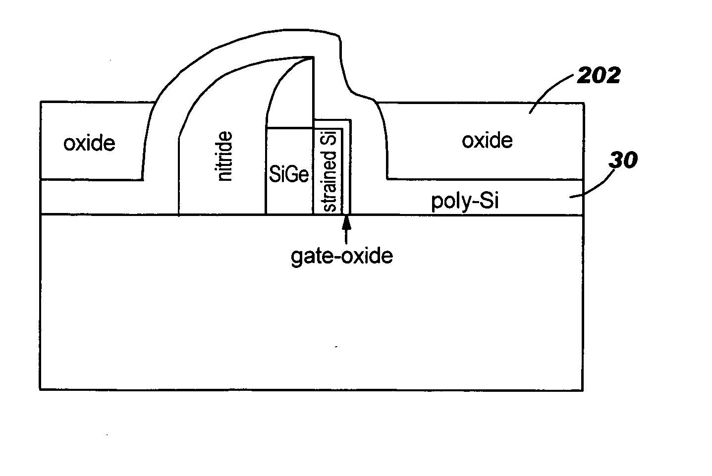
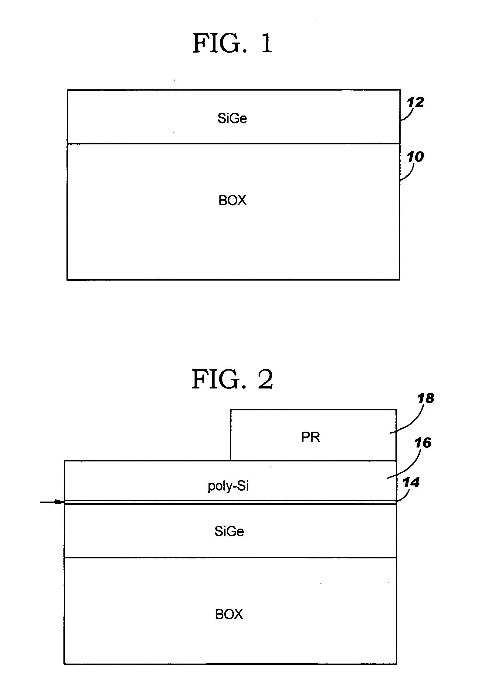
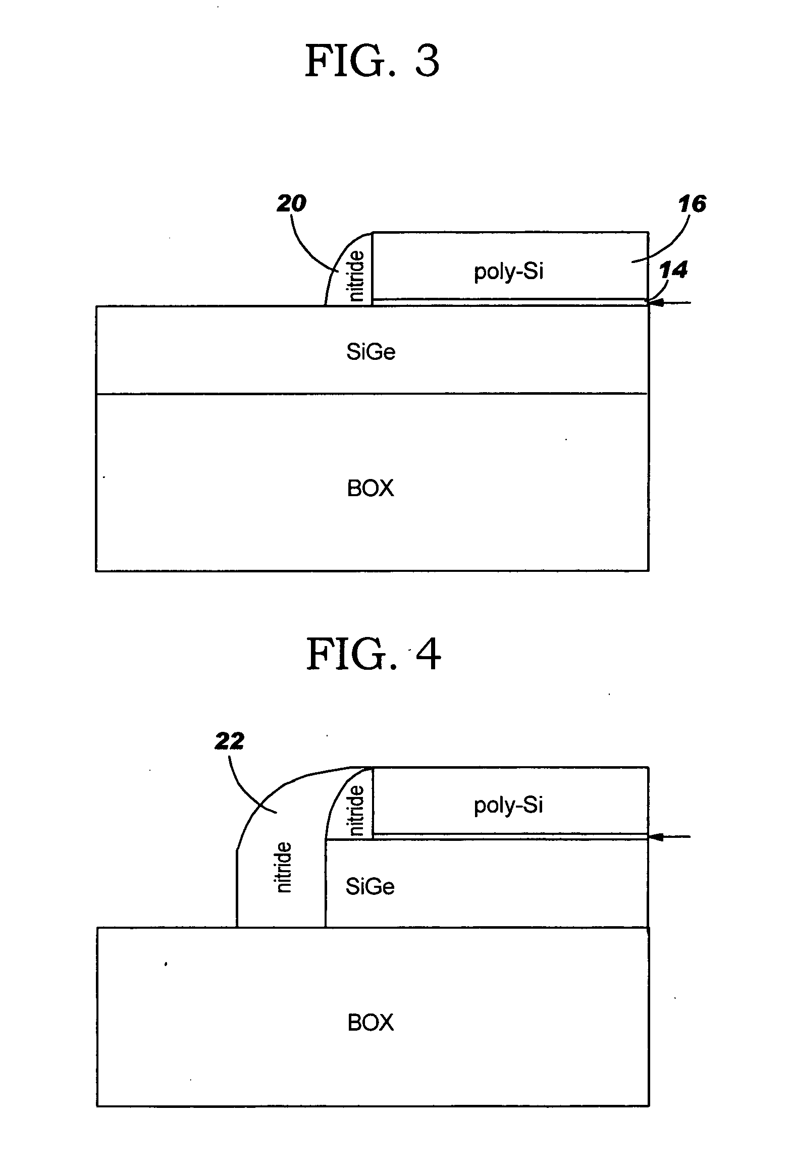
[0015] The invention relates to forming MOSFETs with channels of strained Si. In the invention, transistor performance is enhanced by creating thin films of strained Si. Due to the small dimension of the strained Si, when it is formed, such as by epitaxial growth techniques, the defect density (i.e. dislocation) is typically very low. Such a low defect film may be produced by forming a vertical SiGe bar or block on a relaxed SiGe-on-oxide wafer. One side of the SiGe bar or block may be covered with nitride. The other side of the vertical SiGe bar or block may be covered with a small dimensioned Si film using a selective eptiaxial growth process. The Si film will be strained due to mismatch of the lattice constants with the SiGe substrate. Due to the small dimensions of the Si film and the relaxed structure of the SiGe substrate, the tendency for dislocation formation is reduced. After completion, the strained Si can be subjected to further processing to build various types of MOSFET...


PUM


Abstract

A method and device providing a strained Si film with reduced defects is provided, where the strained Si film forms a fin vertically oriented on a surface of a non-conductive substrate. The strained Si film or fin may form a semiconductor channel having relatively small dimensions while also having few defects. The strained Si fin is formed by growing Si on the side of a relaxed SiGe block. A dielectric gate, such as, for example, an oxide, a high “k” material, or a combination of the two, may be formed on a surface of the strained Si film. Additionally, without substantially affecting the stress in the strained Si film, the relaxed SiGe block may be removed to allow a second gate oxide to be formed on the surface previously occupied by the relaxed SiGe block. Accordingly, a semiconductor device having a strained Si fin vertically oriented on a non-conductive substrate may be formed where the strained Si film is oriented such that it may form a channel of small dimensions allowing access to both sides and top in order to from single gate, double gate, or more gate MOSFETs and finFETs with a channel having a reduced number of defects and/or reduced dimensions.

Description

BACKGROUND OF INVENTION [0001] The invention generally relates to making MOSFETs with vertical gates of strained Si, and more particularly relates to making single gate and double gate MOSFETS and finFETS with vertical gates of strained Si. [0002] As semiconductor devices shrink, traditional device fabrication techniques have approached practical limits in size scaling. For example, as channel lengths shrink below about 50 nm, devices start to exhibit short channel effects including threshold voltage rolling off for shortened channel lengths. Unwanted short channel effects may be reduced by higher doping concentrations, which lead to the unwanted effects of carrier mobility degradation, increased parasitic junction capacitance, and increased sub-threshold swing if doping concentrations become too high. [0003] One method to minimize short channel and reverse short channel effects includes striking an optimum doping profile by well controlled implantation and annealing. However, caref...

Claims


Application Information

Patent Timeline
IPC IPC(8): H01L21/20H01L21/336H01L29/76H01L29/78H01L29/786H01L29/94H01L31/062
CPCH01L29/66795H01L29/78687H01L29/785H01L29/7842
Inventor ZHU, HUILONGBEDELL, STEVEN W.DORIS, BRUCE B.ZHANG, YING
Owner GLOBALFOUNDRIES US INC
Why Eureka
Try Eureka