Exposure apparatus

a technology of exposure apparatus and wafer stage, which is applied in the direction of photomechanical apparatus, instruments, printing, etc., can solve the problems of inability to obtain correct measurement value and large wafer stage, and achieve the effect of good resolution and precise alignment and exposur

Inactive Publication Date: 2005-07-07
CANON KK
View PDF5 Cites 438 Cited by
  • Summary
  • Abstract
  • Description
  • Claims
  • Application Information

AI Technical Summary

Benefits of technology

[0010] Accordingly, it is an exemplary object of the present invention to provide an exposure apparatus that employs a projection optical system that has a high NA (such as an immersion type or 1<NA), and provides precise alignments and exposures with a good resolution without increasing the size of the apparatus.

Problems solved by technology

On the other hand, an image detecting method that images an alignment mark on an image pickup device cannot image the wafer-side pattern on the image pickup device via the projection optical system, or align the reticle-side pattern with the wafer-side pattern.
Therefore, a correct measurement value cannot be obtained due to offsets of the measurement values and the deteriorated measurement reproducibility.
Therefore, disadvantageously, the light having a high NA is reflected on the back surface of the wafer-side reference plate and its light intensity incident upon the light intensity sensor is smaller than that of the light having a small NA.
A non-immersion type exposure apparatus has a similar problem that the light having a large NA is reflected on the back surface of the wafer-side reference plate, due to the higher NA used for the projection optical system.
In order to receive the light having an arbitrary NA, a sensor needs to have a large area and, when a light intensity sensor having a large area is provided on the wafer stage, the wafer stage becomes too large.

Method used


Image

  • Exposure apparatus
  • Exposure apparatus
  • Exposure apparatus

Examples


Embodiment Construction

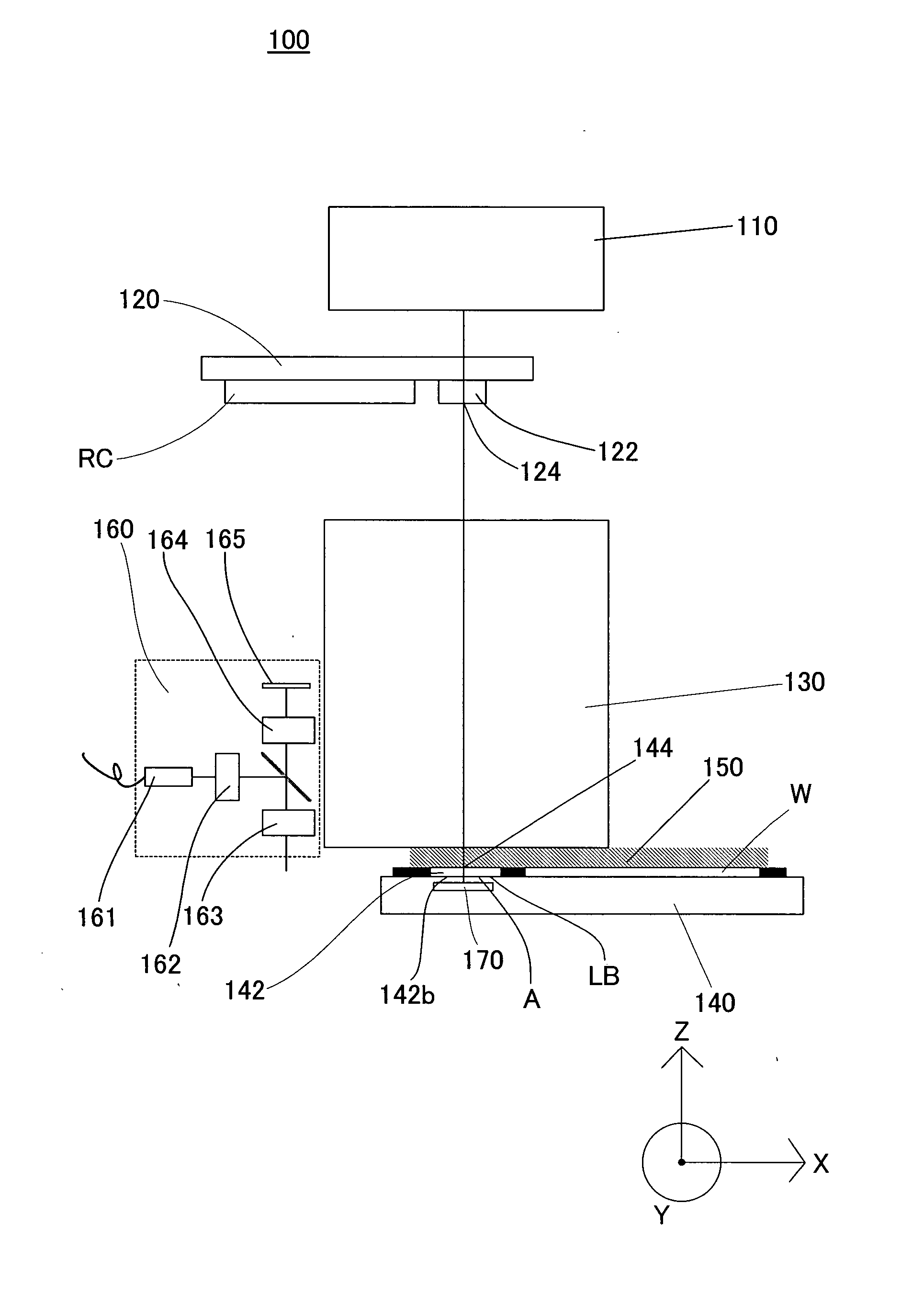
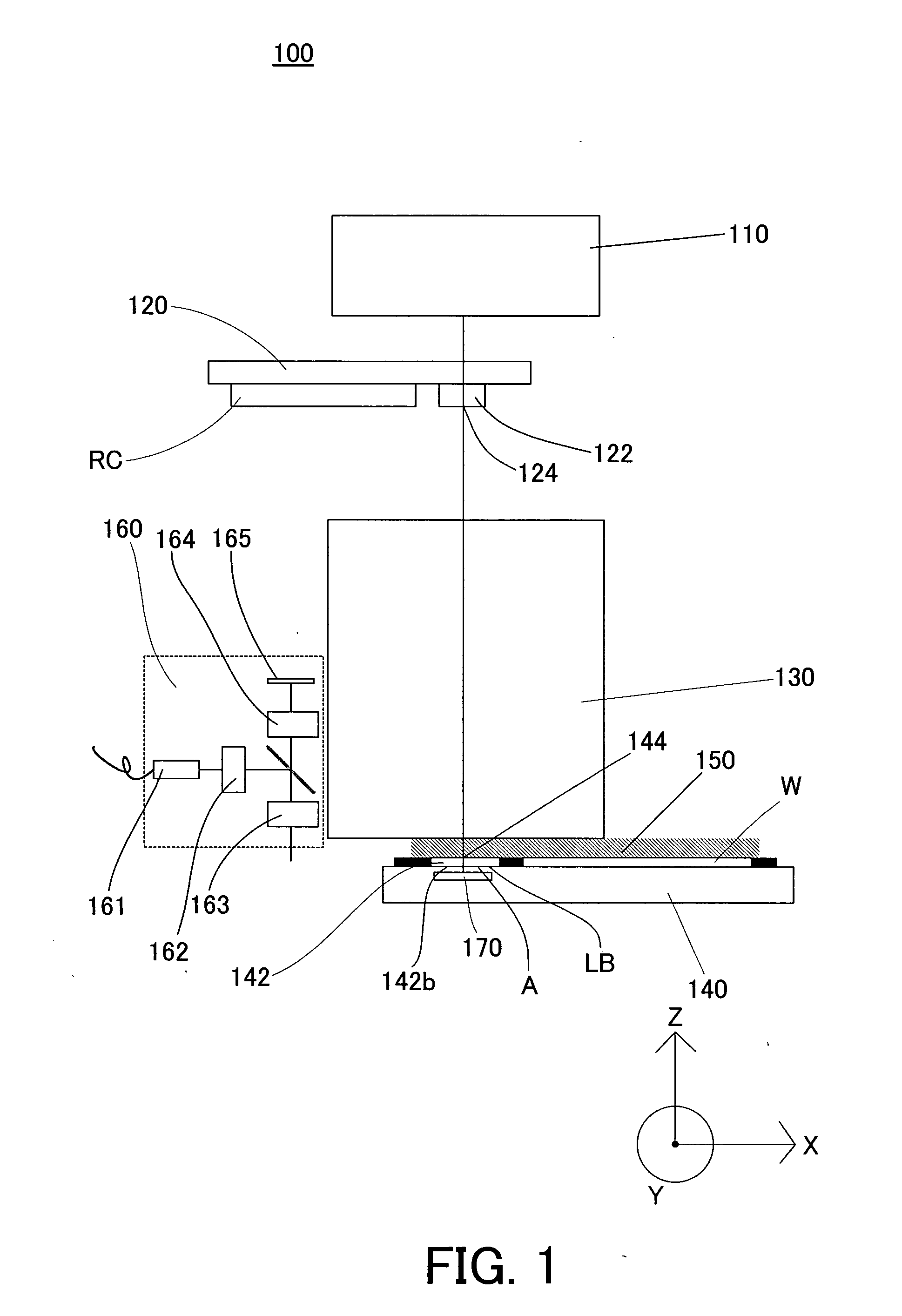
[0033] Referring now to the accompanying drawings, a description will be given of an exposure apparatus according to one aspect of the present invention. A like element in each figure is designated by the same reference numeral, and a duplicate description thereof will be omitted. Here, FIG. 1 is a schematic block diagram of the exposure apparatus 100 according to one aspect of the present invention.

[0034] The exposure apparatus 100 includes, as shown in FIG. 1, an illumination apparatus 110, a reticle stage 120, a projection optical system 130, a wafer stage 140, a fluid 150, an off-axis optical system 160, and a light-receiving element 170. The exposure apparatus 100 is an immersion type exposure apparatus that partially or locally immerses the final surface of the projection optical system 130 at the wafer W side in the fluid 150, and exposes a pattern on a reticle RC onto a wafer W via the fluid 150. The exposure apparatus 100 of the instant embodiment is a step-and-scan projec...


PUM

PropertyMeasurementUnit
refractive indexaaaaaaaaaa
wavelengthaaaaaaaaaa

Abstract

An exposure apparatus includes a projection optical system for projecting a pattern on a reticle onto an object to be exposed, a reference mark that serves as a reference for an alignment between the reticle and the object, a first fluid that has a refractive index of 1 or greater, and fills a space between at least part of the projection optical system and the object and a space between at least part of the projection optical system and the reference mark, and an alignment mechanism for aligning the object by using the projection optical system and the first fluid.

Description

BACKGROUND OF THE INVENTION [0001] The present invention relates generally to an exposure apparatus, and more particularly to an exposure apparatus used to manufacture various devices including semiconductor chips such as ICs and LSIs, display devices such as liquid crystal panels, sensing devices such as magnetic heads, and image pickup devices such as CCDs, as well as fine patterns used for micromechanics. The present invention is suitable, for example, for an immersion type exposure apparatus that immerses, in the fluid, the final surface of the projection optical system and the surface of the object to be exposed, and exposes the object through the fluid. [0002] Conventionally employed reduction projection exposure apparatuses use a projection optical system to project or transfer a circuit pattern on a mask or a reticle onto a wafer, etc., in manufacturing such a fine semiconductor device as a semiconductor memory and a logic circuit in the photolithography technology. [0003] T...

Claims


Application Information

Patent Timeline
Patent Type & Authority Applications(United States)
IPC IPC(8): G03B27/52G03F7/20G03F9/00H01L21/027
CPCG03B27/52G03F9/7096G03F7/7085G03F7/70341
Inventor OHSAKI, YOSHINORI
Owner CANON KK
Why Eureka
Try Eureka