Physically alternating sense amplifier activation

a sense amplifier and physical alternating technology, applied in the field of physical alternating sense amplifier activation scheme, can solve the problems of large waste of space, large rc delay, large bus size, etc., to improve the operation of the device's sense amplifier, reduce the size of the bus, and free up the effect of space in the devi

Inactive Publication Date: 2005-07-07
MICRON TECH INC
View PDF9 Cites 74 Cited by
  • Summary
  • Abstract
  • Description
  • Claims
  • Application Information

AI Technical Summary

Benefits of technology

[0020] The present invention provides a DRAM memory device having relatively large sense amplifier drivers (i.e., RNL* and ACT drivers), which improve the operation of the device's sense amplifiers, reduce the size of the buses used for the sense amplifier activation signals and free up space in the device for additional functionality.
[0021] The above and other features and advantages are achieved by a memory device having banks of sense amplifiers comprising two types of sense amplifiers. A first driver used to activate the first type of sense amplifier is embedded into a first bank. A second driver used to activate a second type of sense amplifier is embedded into a second bank. No sense amplifier driver circuitry is contained within gaps or min-gaps between the banks of sense amplifiers. This alternating physical placement of the first and second sense amplifier drivers within respective banks is repeated throughout the device. This alternating physical arrangement frees up the gaps and mini-gaps for other functions, reduces the buses used for sense amplifier activation signals and allows large drivers to be used, which improves the operation of the sense amplifiers and the device itself.

Problems solved by technology

If the word line is too long, then the RC delay becomes prohibitive.
This scheme, however, requires large sense amplifiers and circuitry in the gaps.
This space requirement between the n-channel and p-channel transistors (if implemented adjacent each other) is a large wasteful area that could have been used for additional driver width.
Having the drivers in different gaps reduces this problem, but it is not an optimal solution particularly in light of new DRAM architectures.
This forces the designer of the DRAM 140 to use inadequate sense amplifier drivers or to waste precious space on the chip to implement adequate ones.

Method used


Image

  • Physically alternating sense amplifier activation
  • Physically alternating sense amplifier activation
  • Physically alternating sense amplifier activation

Examples


Embodiment Construction

[0035] In the following detailed description, reference is made to various specific embodiments in which the invention may be practiced. These embodiments are described with sufficient detail to enable those skilled in the art to practice the invention, and it is to be understood that other embodiments may be employed, and that structural and electrical changes may be made without departing from the spirit or scope of the present invention.

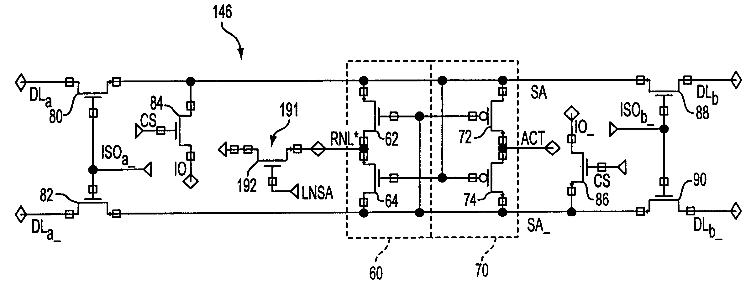
[0036] As set forth above, there is a desire and need to implement adequately sized ACT and RNL* drivers in a DRAM device. Proper sizing of these drivers will improve sense amplifier operation and operation of the DRAM device itself. It is also desirable to implement these drivers without wasting precious space in the device.

[0037] One possible solution is to embed both the ACT and RNL* drivers into each sense amplifier of the banks of sense amplifiers. Although it would be possible to obtain larger drivers, this scheme would take up an enormous...


PUM


Abstract

A memory device having banks of sense amplifiers comprising two types of sense amplifiers. A first driver used to activate the first type of sense amplifier is embedded into a first bank. A second driver used to activate a second type of sense amplifier is embedded into a second bank. This alternating physical placement of the first and second sense amplifier drivers within respective banks is repeated throughout the device. This alternating physical arrangement frees up the gaps and mini-gaps for other functions, reduces the buses used for sense amplifier activation signals and allows large drivers to be used, which improves the operation of the sense amplifiers and the device itself.

Description

FIELD OF THE INVENTION [0001] The present invention relates to the field of semiconductor memory devices and, more particularly to a physically alternating sense amplifier activation scheme for a semiconductor memory device. BACKGROUND OF THE INVENTION [0002] An essential semiconductor device is semiconductor memory, such as a random access memory (RAM) device. A RAM device allows the user to execute both read and write operations on its memory cells. Typical examples of RAM devices include dynamic random access memory (DRAM) and static random access memory (SRAM). [0003] DRAM is a specific category of RAM containing an array of individual memory cells, where each cell includes a capacitor for holding a charge and a transistor for accessing the charge held in the capacitor. The transistor is often referred to as the access transistor or the transfer device of the DRAM cell. [0004]FIG. 1 illustrates a portion of a DRAM memory circuit containing two neighboring DRAM cells 10. Each cel...

Claims


Application Information

Patent Timeline
Patent Type & Authority Applications(United States)
IPC IPC(8): G11C7/06G11C7/08G11C11/4091
CPCG11C7/06G11C11/4091G11C7/065
Inventor SCHRECK, JOHN
Owner MICRON TECH INC
Why Eureka
Try Eureka