

Semiconductor test device
a test device and semiconductor technology, applied in the direction of measurement devices, electronic circuit testing, instruments, etc., can solve the problems of inability to test a high-speed device which outputs output data with a timing of this internal clock, inability to acquire output data with edge timings of the device under test, and inability to conduct test with respect to the device. achieve the effect of high multi-usability and convenien
- Summary
- Abstract
- Description
- Claims
- Application Information
AI Technical Summary
Benefits of technology
Problems solved by technology
Method used
Image

Examples
first embodiment
[0061] A first embodiment of a semiconductor test apparatus according to the present invention will now be described with reference to FIGS. 1 to 6.
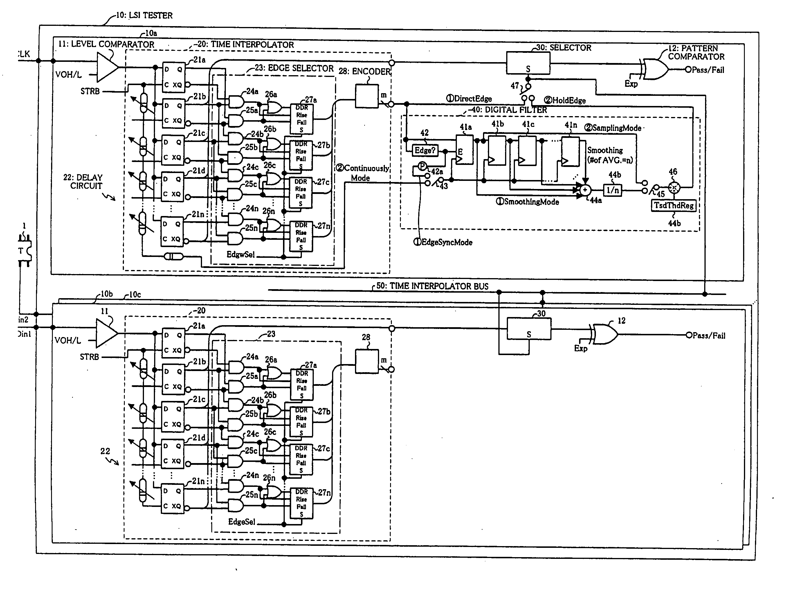
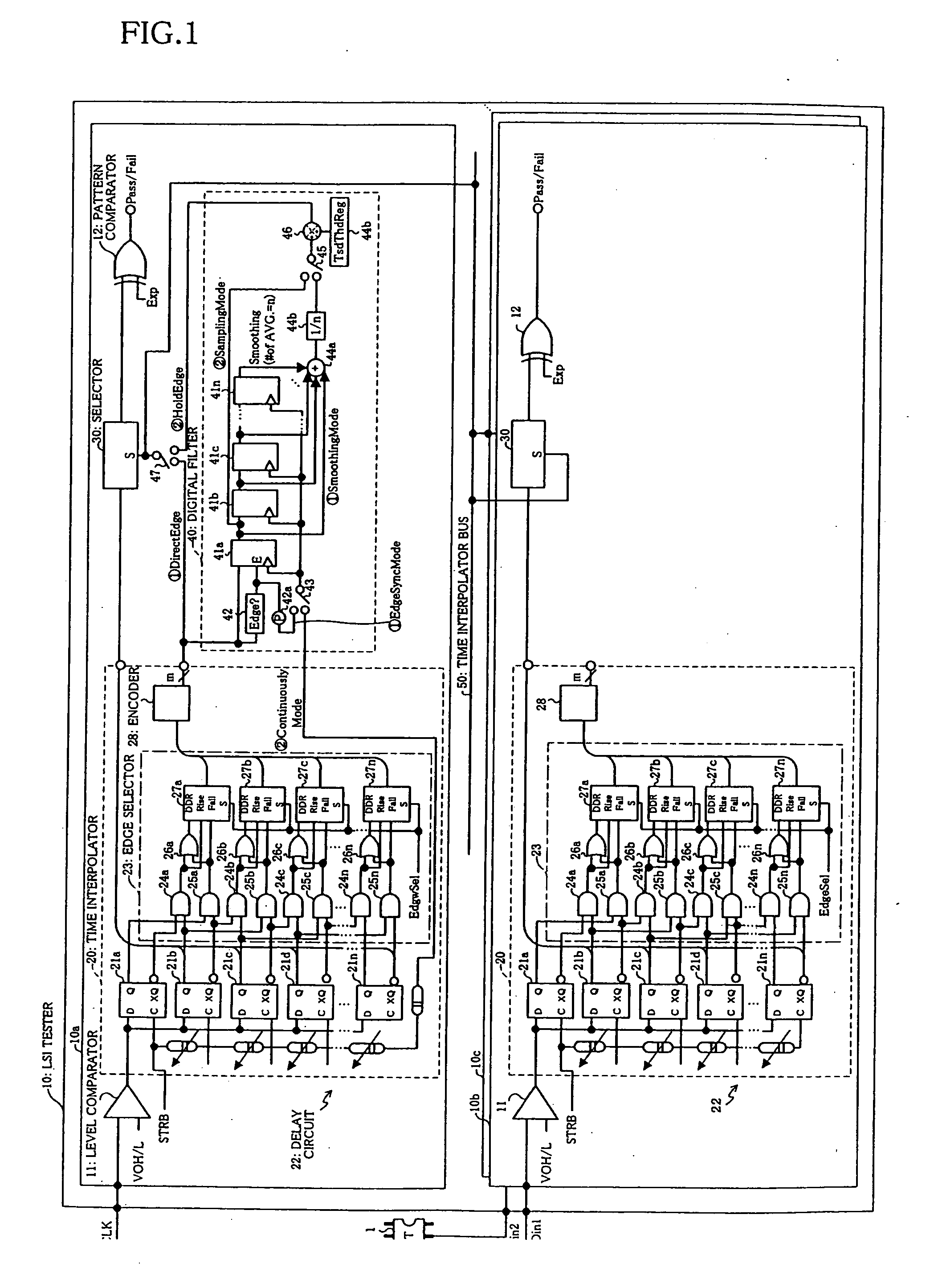
[0062]FIG. 1 is a block diagram showing a structure of a semiconductor test apparatus according to a first embodiment of the present invention. As shown in the drawing, the semiconductor test apparatus according to this embodiment comprises an LSI tester 10 which conducts a function test of a device under test (DUT) 1, the LSI tester 10 acquires output data output from the device under test 1 as measurement data, and the acceptability of the device under test 1 is judged by comparing the measurement data with predetermined expectation value data.
[0063] The device under test 1 outputs predetermined output data upon receiving a signal from a non-illustrated pattern generator or the like, and outputs a clock signal (system clock).
[0064] As the LSI which outputs clocks therefrom in this manner, for example, there is the above-described LS...
embodiments
[0187] Concrete embodiments will now be described hereinafter with reference to FIGS. 2 to 6.
[Basic Operation in Hold Edge Mode]
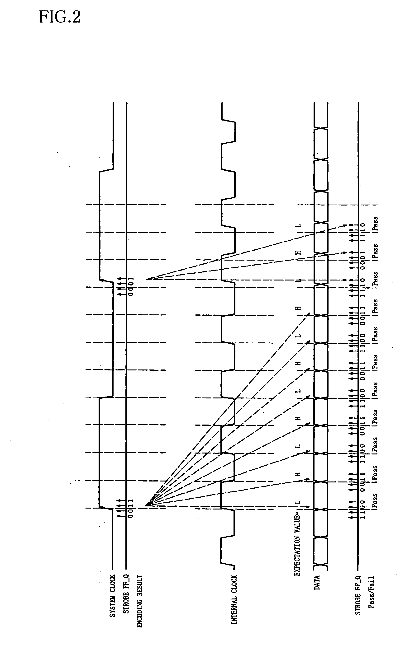
[0188] First, a description will be given as to a basic operation when obtaining output data of the device under test 1 by using a recovery clock acquired by the digital filter 40 in the semiconductor test apparatus according to this embodiment with reference to FIG. 2. FIG. 2 is a signal diagram showing an operation example of the Hold Edge mode to obtain output data which is output in accordance with an internal clock with a timing of a recovery clock obtained from a system clock of the device under test 1.
[0189] In the example shown in FIG. 2, the device under test 1 is an ODR type device from which data is output in synchronization with both a rise edge and a fall edge of the internal clock having a frequency which is fourfold of that of the system clock, and output data is output at a data rate which is eightfold of that of the system clock. Therefo...
second embodiment
[0228] A second embodiment of the semiconductor test apparatus according to the present invention will now be described with reference to FIG. 7.
[0229]FIG. 7 is a block diagram showing a structure of a semiconductor test apparatus according to the second embodiment of the present invention. As shown in the drawing, the semiconductor test apparatus according to this embodiment is a modified embodiment of the above-described first embodiment, and a jitter detection circuit 60 is further provided to the source synchronous circuit (clock recovery circuit) 10a on the clock side in the first embodiment.
[0230] Therefore, any other constituent part is the same as that in the first embodiment, and like reference numerals denote like constituent parts, thereby eliminating the detailed explanation.
[0231] The jitter detection circuit 60 receives positional data which can be a reference of the recovery clock output from the registers 41a to 41n of the digital filter 40 and detects a phase dif...
PUM
 Abstract
Description
Claims
Application Information