Metallic thin film piezoresistive transduction in micromechanical and nanomechanical devices and its application in self-sensing SPM probes

a technology of piezoresistive transduction and metal thin film, applied in the direction of piezo-resistive materials, force measurement, mechanical roughness/irregularity measurement, etc., can solve the problems of complex and expensive fabrication process of semiconducting piezoresistors, such as ion implantation or molecular beam epitaxy, and relative large thermal noise floor

Inactive Publication Date: 2005-07-14
CALIFORNIA INST OF TECH
View PDF33 Cites 52 Cited by
  • Summary
  • Abstract
  • Description
  • Claims
  • Application Information

AI Technical Summary

Problems solved by technology

Doped silicon has a fairly high gauge factor (20˜100), but also high sheet resistance (10 kOhm/square) and therefore a relatively large thermal noise floor.
Much higher 1/f noise is also expected in doped silicon due to its low carrier density.
Additionally, fabrication...

Method used


Image

  • Metallic thin film piezoresistive transduction in micromechanical and nanomechanical devices and its application in self-sensing SPM probes
  • Metallic thin film piezoresistive transduction in micromechanical and nanomechanical devices and its application in self-sensing SPM probes
  • Metallic thin film piezoresistive transduction in micromechanical and nanomechanical devices and its application in self-sensing SPM probes

Examples


application examples

Device Application Examples

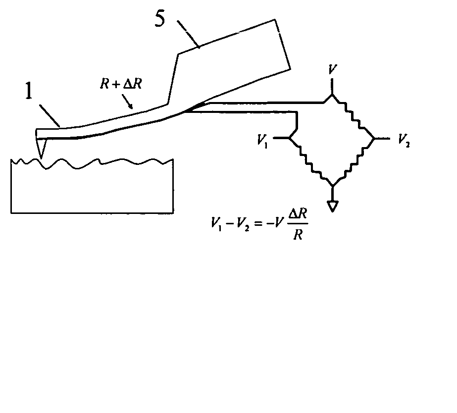
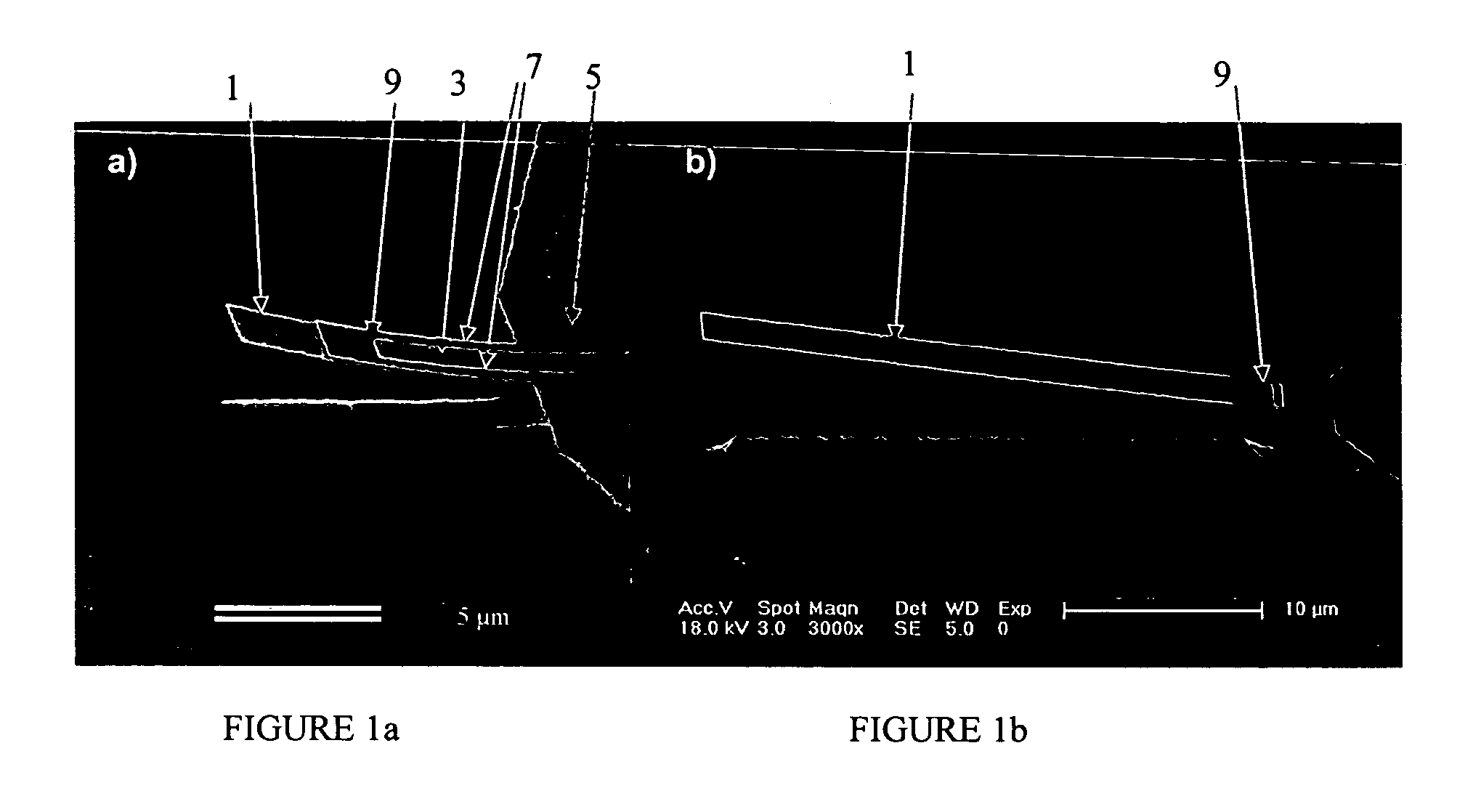
[0043]FIGS. 5a and 5b illustrate an example of the use of the metal films in self-sensing cantilever probes for atomic force microscopes. FIG. 5a is a schematic and FIG. 5b is an SEM image of a micromachined cantilever (i.e., probe) 11 with the following micro-scale dimensions: 150 μm long×30 μm wide×4 μm thick. The probe 11 contains the cantilever 1, the notch 3, base 5, legs 7, metal film 9 and a sharp AFM tip 13. Preferably, but not necessarily, the metal film 9 is formed on the same side of the cantilever as the tip 13. The specific probe 11 shown in FIG. 5 is designed for tapping-mode AFM. Probes for contact mode AFM can be designed as well, but with much smaller spring constants, as will be described in more detail below.

[0044]FIGS. 12 and 13 illustrate the fabrication processes for both non-contact mode probes 11 and contact mode probes 21, respectively. As shown in FIGS. 12a-h, a method for making non-contact / tapping mode piezoresistive SPM probes...


PUM


Abstract

Thin metallic films are used as the piezoresistive self-sensing element in microelectromechanical and nanoelectromechanical systems. The specific application to AFM probes is demonstrated.

Description

CROSS-REFERENCE TO RELATED APPLICATIONS [0001] This application is a continuation-in-part of U.S. application Ser. No. 10 / 826,007 filed Apr. 16, 2004, which claims benefit of priority of U.S. Provisional application Ser. No. 60 / 468,452, filed May 7, 2003. This application also claims benefit of priority of U.S. Provisional Application Ser. No. 60 / 562,652, filed Apr.15, 2004. All of the above mentioned applications are incorporated herein by reference in their entirety.BACKGROUND OF THE INVENTION [0002] 1. Field of the Invention [0003] This invention is related to piezoresistive sensors for micro-electro-mechanical systems (MEMS) and nano-electro-mechanical systems (NEMS). [0004] 2. Description of the Prior Art [0005] Piezoresitive displacement detection techniques are attractive in both microelectromechanical and nanoelectromechanical systems (MEMS and NEMS), because they can be fully integrated and are easy to use. Applications include scanning probe microscopy, force and pressure ...

Claims


Application Information

Patent Timeline
IPC IPC(8): G01L1/18G01L1/20
CPCB82Y35/00G01L1/18G01L1/20G01Q60/38G01N33/54373G01Q20/04G01N33/54346
Inventor TANG, HONGXINGLI, MOROUKES, MICHAEL L.
Owner CALIFORNIA INST OF TECH
Why Eureka
Try Eureka