

Method for reducing wiring congestion in a VLSI chip design
a technology of integrated circuits and circuit designs, applied in computer aided design, semiconductor/solid-state device details, instruments, etc., can solve problems such as inability to perform the desired function, and inability to guarantee the box's function, so as to avoid the congestion of wiring areas and never degrade the effect of wiring congestion
- Summary
- Abstract
- Description
- Claims
- Application Information
AI Technical Summary
Benefits of technology
Problems solved by technology
Method used
Image

Examples
Embodiment Construction
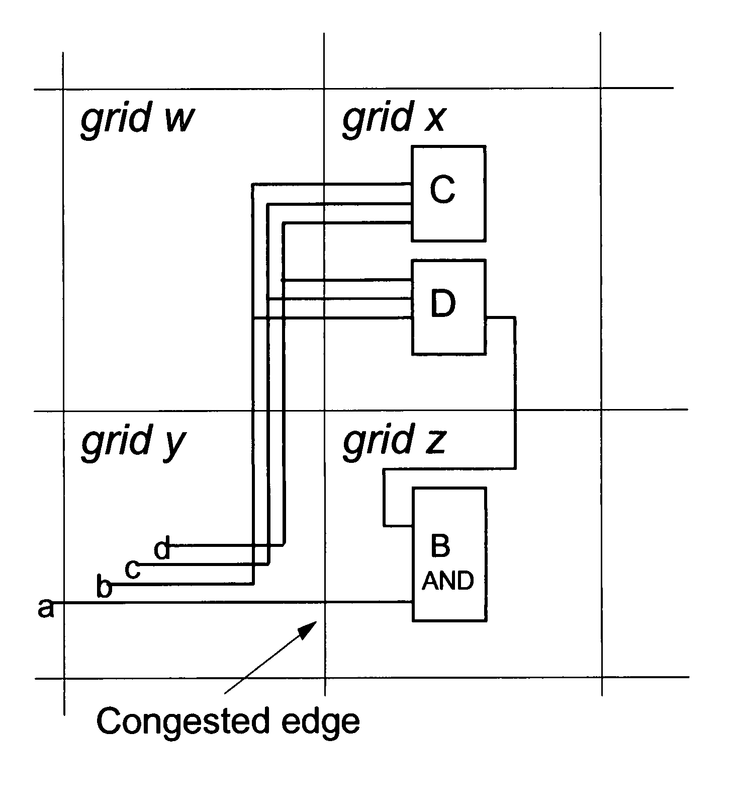
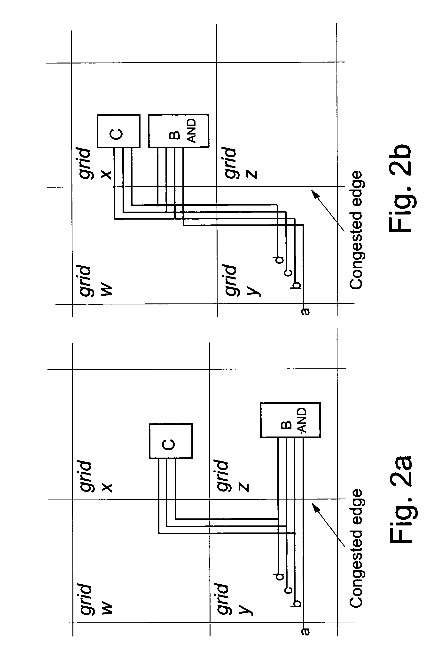
[0043] The novelty of the invention being described herein resides in applying transformations that move, decompose, add logic elements or modify wire connections in order to reduce congestion and provide a routable design. Hereinafter, an algorithm is provided along with incremental placement and incremental routing to relieve the wiring congestion. Success at this process reduces or eliminates the need for manual intervention on the part of the designer.
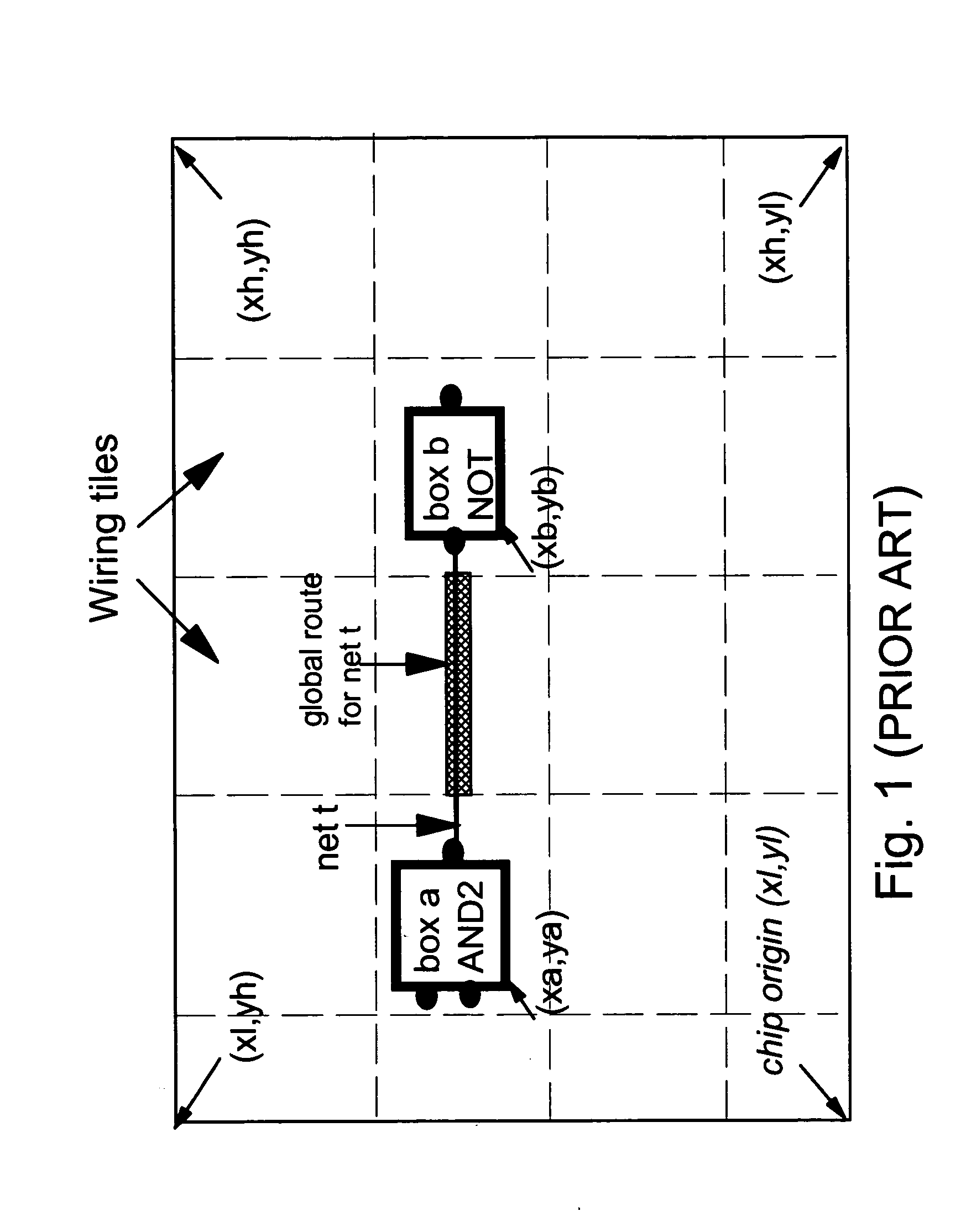
[0044] The method assumes that the design is already placed, optimized and globally routed. Global routing places a wiring grid over the design, as described above. Each edge of the grid has a known capacity which is the amount of wire Ci that can pass over edge I, and a utilization Ui, (i.e., how many wires cross the edge i, weighted by width), such that
Ui=Sumwire j crossing edge i widthj, (Eq. 1)
wherein widthj is the width of wire j crossing edge i. (In the present example, for clarity sake, all the wires are assumed to hav...
PUM
 Abstract
Description
Claims
Application Information