Fabrication process for a semiconductor integrated circuit device

a technology of integrated circuit device and fabrication process, which is applied in the direction of semiconductor devices, semiconductor/solid-state device details, electrical apparatus, etc., can solve the problems of not fully establishing the total image including the structure and fabrication, becoming difficult to bury the connecting hole, and difficult to bury copper in the connecting hole by the sputtering method, etc., to improve the reliability of the buried interconnection

Inactive Publication Date: 2005-07-14
HITACHI LTD
View PDF20 Cites 16 Cited by
  • Summary
  • Abstract
  • Description
  • Claims
  • Application Information

AI Technical Summary

Benefits of technology

[0008] An object of the present invention is therefore to provide, in a semiconductor integrated circuit device having a buried interconnection structure, a technique for favorably burying a conductor film for buried interconnection without using a highly-advanced technique.
[0010] A further object of the present invention is to provide a technique for improving the reliability of a buried interconnection.
[0011] A still further object of the present invention is to provide a technique for introducing a copper-conductor material-buried interconnection in the whole structure of a semiconductor integrated circuit device without causing any inconvenience.

Problems solved by technology

More specifically, the problem is that no total image including the structure and fabrication has yet been established completely in the case where the technique for forming a buried interconnection is applied to a semiconductor integrated circuit device.
Particularly, in the dual damascene method, an interconnection-forming groove and connecting hole are buried with the same conductor film at the same time Owing to the miniaturization of the interconnection or connecting hole, however, it becomes difficult to-bury the connecting hole, which is more minute than the interconnection-forming groove, simultaneously with the interconnection-forming groove, while maintaining good electrical properties sufficiently.
When copper is employed as a wiring material, it is difficult to bury copper in the connecting hole by the sputtering method.
In addition, the burying capacity of the plating method is not freely high, and the burying of a minute connecting hole having a high aspect ratio is difficult to achieve.
Such a problem also appears when interconnection grooves with different aspect ratios exist in the same interconnection film to be buried.

Method used


Image

  • Fabrication process for a semiconductor integrated circuit device
  • Fabrication process for a semiconductor integrated circuit device
  • Fabrication process for a semiconductor integrated circuit device

Examples


first embodiment

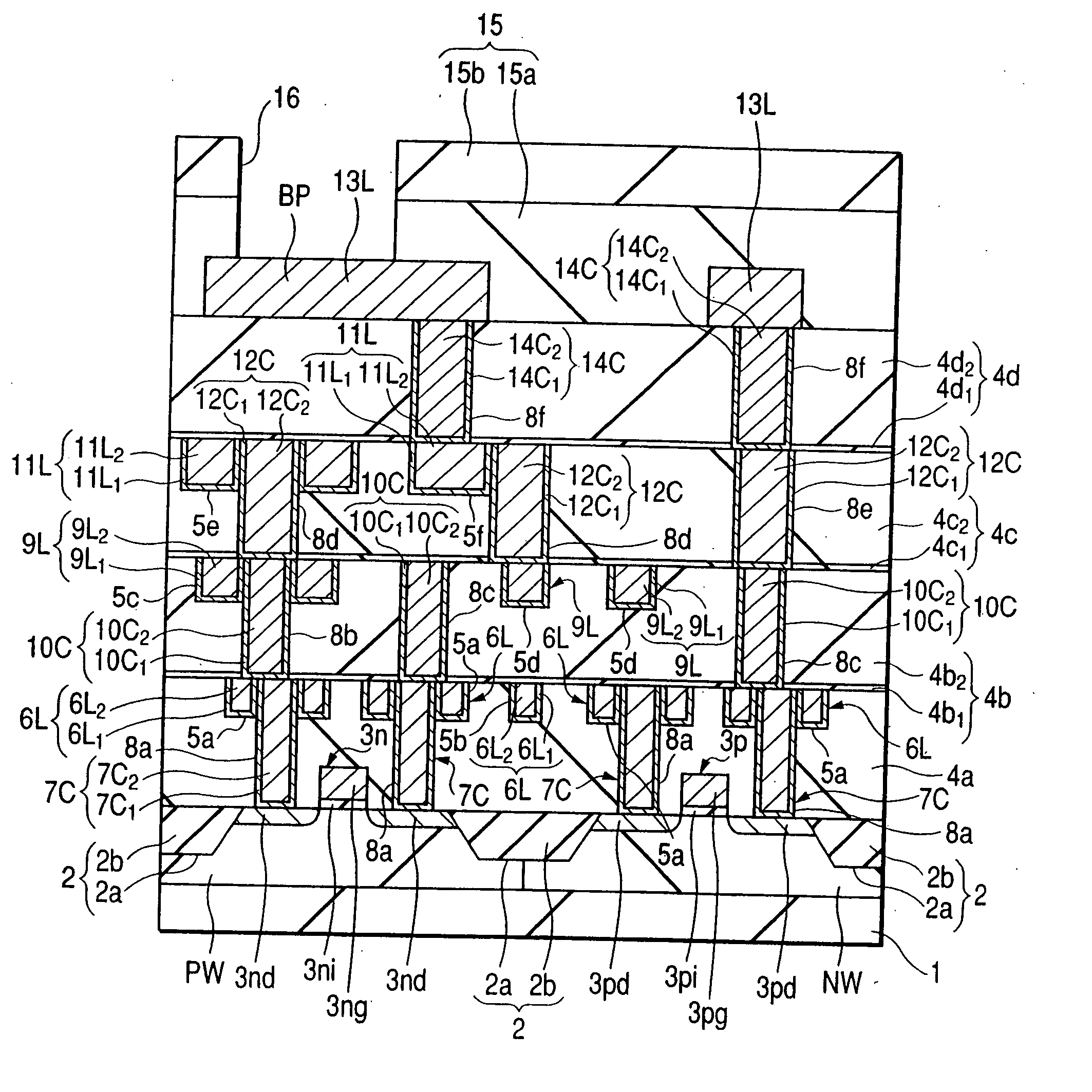
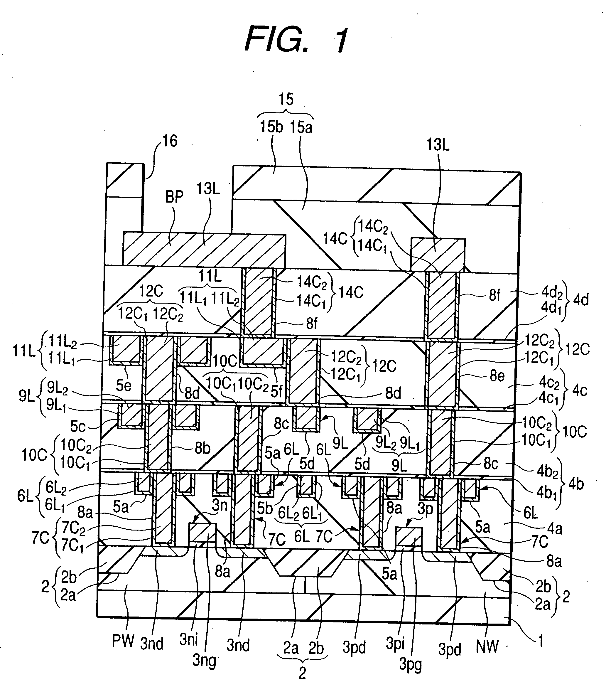
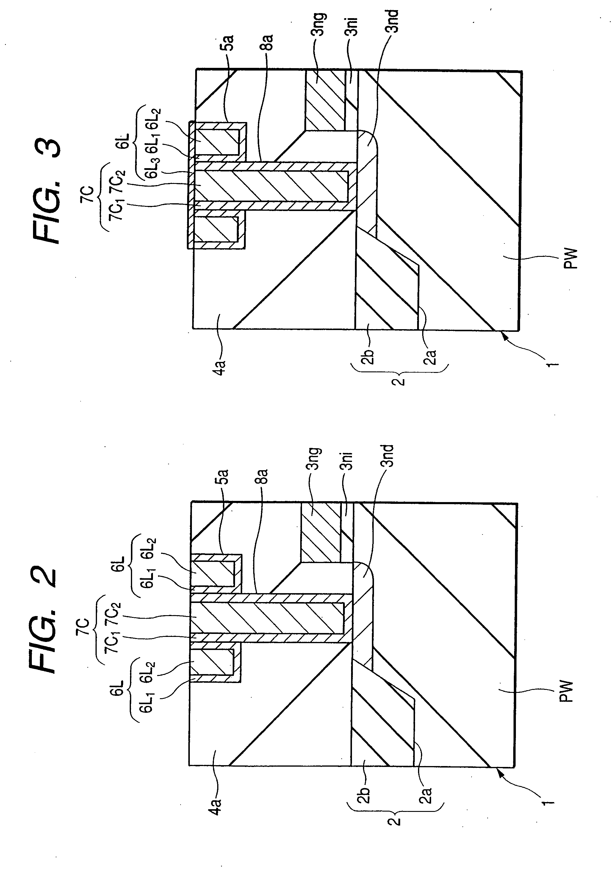
[0097]FIG. 1 is a fragmentary cross-sectional view of the semiconductor integrated circuit according to the first embodiment of the present invention; FIG. 2 is a fragmentary cross-sectional view illustrating the first-layer interconnection of the semiconductor integrated circuit device of FIG. 1; FIGS. 3 through 5 are cross-sectional views illustrating a modification of the interconnection structure of FIG. 2; FIG. 6 is a fragmentary cross-sectional view illustrating the second-layer interconnection of the semiconductor integrated circuit device of FIG. 1; FIG. 7 is a fragmentary cross-sectional view illustrating a modification of the connection between interconnection layers of the semiconductor integrated circuit device of FIG. 1; FIGS. 8 through 12 are fragmentary cross-sectional views of the semiconductor integrated circuit device of FIG. 1 during its fabrication process; and FIGS. 13 through 18 are fragmentary, partially-cutaway, perspective view of the semiconductor integrate...

second embodiment

[0189]FIGS. 19 through 23 are fragmentary cross-sectional views of the semiconductor integrated circuit device according to the second embodiment of the present invention during the fabrication process and FIG. 24 is a fragmentary cross-sectional view illustrating the semiconductor integrated circuit device.

[0190] This second embodiment is different from the first embodiment in the structure of a connecting conductor portion and its forming process.

[0191] As illustrated in FIG. 19, a photoresist pattern 17b is formed on the upper surface of the interlayer insulating film 4a for the formation of an interconnection groove. Then, the interlayer insulating film 4a is etched with the photoresist pattern 17b as an etching mask, whereby an interconnection groove 5a is formed in the upper part of the interlayer insulating film 4a.

[0192] After the removal of the photoresist pattern 17b, a photoresist pattern 17c is formed, as illustrated in FIG. 20, over the interlayer insulating film 4a ...

third embodiment

[0201]FIGS. 25 through 28 and FIGS. 29 through 32 are fragmentary cross-sectional views of the semiconductor integrated circuit device according to the third embodiment of the present invention during the fabrication process; and FIG. 33 is a fragmentary cross-sectional view of the semiconductor integrated circuit device.

[0202]FIG. 25 illustrates the semiconductor integrated circuit device during the fabrication process. In the interlayer insulating film 4a, the interconnection groove 5a and connecting hole 8a are formed by the method as described in the second embodiment.

[0203] In the third embodiment, the connecting conductor portion 7C made of, for example, tungsten is formed in the connecting hole 8a by the selective CVD method as illustrated in FIG. 26. In this third embodiment, the film formation is carried out to such an extent as the upper part of the connecting conductor portion 7C protrudes outside the interconnection groove 5a. The material of the connecting conductor p...


PUM

PropertyMeasurementUnit
depthaaaaaaaaaa
depthaaaaaaaaaa
aspect ratioaaaaaaaaaa

Abstract

In a fabrication process of a semiconductor integrated circuit device, upon effecting connection of an interconnection made of aluminum or aluminum alloy and another interconnection made of Cu or Cu alloy, a barrier conductor film or plug is disposed at the joint portion between these interconnections. Among the interconnection layers formed, the uppermost one is made of a wiring material such as aluminum or aluminum alloy, while the lower one is made of Cu or Cu alloy. The lowest interconnection is made of a conductive material other than Cu or Cu alloy. For example, the conductive material which permits minute processing and has both low resistance and high EM resistance such as tungsten is employed.

Description

[0001] This is a divisional of U.S. application Ser. No. 10 / 797,017, filed Mar. 11, 2004, which, in turn, is a continuation of U.S. application Ser. No. 09 / 613,138, filed Jul. 10, 2000 (now U.S. Pat. No. 6,731,007), and which, in turn, is a continuation of U.S. application Ser. No. 09 / 139,410 filed Aug. 25, 1998 (now abandoned), the entire disclosures of which are incorporated herein by reference.BACKGROUND OF THE INVENTION [0002] This invention relates to a semiconductor integrated circuit device and a technique for fabrication thereof, particularly to a technique which is effective when applied to an interconnection-forming technique for a semiconductor circuit. [0003] As an interconnection forming process for a semiconductor integrated circuit, there is a process, for example, called a Damascene process. In this process, a buried interconnection is formed in an interconnection-forming groove by making an interconnection-forming groove in an insulating film, depositing an intercon...

Claims


Application Information

Patent Timeline
Patent Type & Authority Applications(United States)
IPC IPC(8): H01L21/768H01L23/485H01L23/522H01L23/528H01L23/532
CPCH01L21/76838H01L21/76843H01L2924/1305H01L2924/13091H01L2924/01021H01L24/48H01L2924/04941H01L21/7685H01L21/76877H01L21/76882H01L23/485H01L23/5226H01L23/5283H01L23/53228H01L2224/05624H01L2224/48463H01L2924/01012H01L2924/01013H01L2924/01029H01L2924/01078H01L2924/01079H01L2924/00014H01L2924/00H01L2924/14H01L2224/02166H01L21/76807H01L21/76885H01L21/76847H01L21/76852H01L2224/45099H01L2224/45015H01L2924/207
Inventor SAITO, TATSUYUKINOGUCHI, JUNJIYAMAGUCHI, HIZURUOWADA, NOBUO
Owner HITACHI LTD
Why Eureka
Try Eureka