Check patentability & draft patents in minutes with Patsnap Eureka AI!

Semiconductor memory having variable memory size and method for refreshing the same

Active Publication Date: 2005-07-14
SAMSUNG ELECTRONICS CO LTD
View PDF4 Cites 19 Cited by
  • Summary
  • Abstract
  • Description
  • Claims
  • Application Information

AI Technical Summary

Benefits of technology

[0016] According to yet another aspect of the present invention, a method is provided of refreshing a semiconductor memory device operable in a full memory capacity mode and N reduced memory capacity modes, where N is an integer of 1 or more, the memory device including a memory array comprising 2N memory blocks each having at least one word line, where m is an integer of 2N or more. The method includes generating a refresh reference signal pulse having a period T, generating a first n-bit address signal having bits A0, A1, . . . , An, where n is an integer greater than or equal to N, and where a logic value of the n-bit address signal is sequentially incremented by 1 at each period T of the refresh reference pulse signal. The method further includes generating a refresh main signal according to a mode control signal and bits A0 . . . A(N−1) of the first address signal, and generating a second n-bit address signal having bits R0, R1, . . . , Rn, where the second parallel n-bit address signal is generated at a timing of the refresh main signal, where the bits A0 . . . A(N−1) of the first parallel n-bit address signal are respectively output as the bits Rn . . . R(n-(N−1)) of the second n-bit address signal, and where the bits A(N) . . . An of the first n-bit address signal are respectively output as the bits R0 . . . R(n-(N−2)) of the second n-bit parallel signal. A word line of the memory array is addressed according to the second n-bit parallel signal at a timing of the refresh main signal.

Problems solved by technology

As is best explained by way of example, this refresh requirement creates a problem when the RMS mode is used.
A problem arises in this case because the effective refresh cycle time for the fourth word line (3) is 12T during the transition between memory modes.
This exceeds the design refresh cycle time of 8T, meaning that data contained in the memory cells of the fourth word line can be lost.
As shown in FIG. 2, this problem also arises when switching from the half memory mode to the full memory mode.

Method used


Image

  • Semiconductor memory having variable memory size and method for refreshing the same
  • Semiconductor memory having variable memory size and method for refreshing the same
  • Semiconductor memory having variable memory size and method for refreshing the same

Examples


Embodiment Construction

[0031] The present invention will now be described in detail with reference to several non-limiting preferred embodiments.

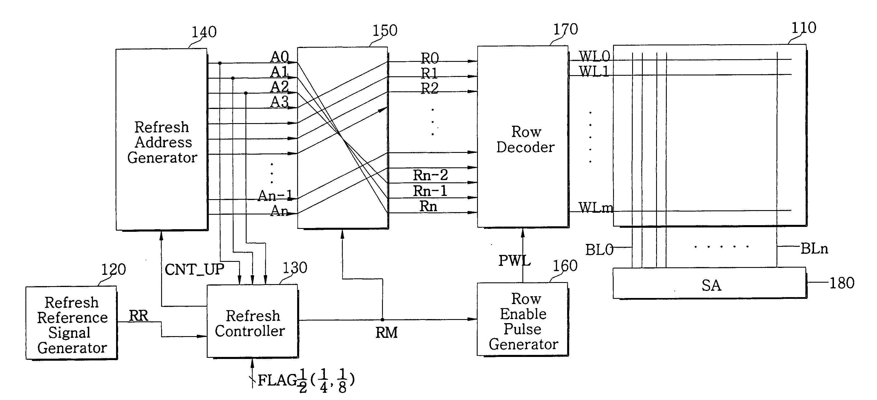
[0032] A semiconductor memory device according to one non-limiting embodiment of the present invention will be described with reference to FIGS. 3, 4 and 5. This embodiment is capable of selectively operating in one of four memory modes, i.e., a full memory mode, a half (½) memory mode, a quarter (¼) memory mode, and an eighth (⅛) memory mode.

[0033] As shown, the memory device of FIG. 3 includes a memory array 110, refresh reference signal generator circuit 120, a refresh controller 130, a refresh address generator circuit 140, an address sorter circuit 150, a row enable pulse generator circuit 160, a row decoder circuit 170, and a sense amplifier (SA) circuit 180.

[0034] The memory array 110 is connected to a plurality of bit lines BL0-BLn, which in turn are connected to the sense amplifier 180. Further, as schematically illustrated in FIG. 4, the memory array...


PUM


Abstract

A semiconductor memory device is operable in a full capacity mode and at least one reduced capacity mode, and includes a memory array having a plurality of memory blocks, each of the memory blocks having at least one word line. An address generation circuit generates a first multi-bit address signal having a logic value which is sequentially incremented by one during each of successive refresh periods. An address sorting circuit receives the first multi-bit address signal and outputs a second multi-bit address signal in which one or more least significant bits of the first multi-bit address signal are arranged in the second multi-bit address signal to indicate a memory block of the memory array, and in which remaining bits of the first multi-bit address signal are arranged in the second multi-bit address to indicate a word line within the selected memory block. The word lines of the memory array are refreshed according to the second multi-bit address signal.

Description

BACKGROUND OF THE INVENTION [0001] 1. Field of the Invention [0002] The present invention generally relates to semiconductor memories and to methods of refreshing memory cells of semiconductor memories. More particularly, the present invention relates to semiconductor memories having variable memory sizes and to methods of refreshing memory cells of such memories. [0003] 2. Description of the Related Art [0004] Variable sized semiconductor memory devices are known in which all or a subset of the memory blocks contained in the devices can be selectively utilized. One such memory device is the Uni-transistor RAM (UtRAM), also known as the Psuedo SRAM (PSRAM), which is configured of DRAM cells but has an SRAM interface. For example, a 16 mega-bit (16 M) UtRAM operating in a full memory mode can function like a 16 M SRAM, whereas the same 16 M UtRAM operating in a half memory mode can function like an 8 M SRAM. [0005] Largely for cost reasons, it is sometimes preferable to implement an ...

Claims


Application Information

Patent Timeline
IPC IPC(8): G11C7/10G11C11/401G11C11/406
CPCG11C7/1045G11C11/40622G11C11/406G11C11/401
Inventor LEE, YOU-MINAM, KYUNG-WOO
Owner SAMSUNG ELECTRONICS CO LTD
Features
  • R&D
  • Intellectual Property
  • Life Sciences
  • Materials
  • Tech Scout
  • Unparalleled Data Quality
  • Higher Quality Content
  • 60% Fewer Hallucinations
Learn More