Liquid crystal display device

a liquid crystal display and liquid crystal technology, applied in the field of active matrix type can solve the problems of affecting the display effect of liquid crystal display devices

Active Publication Date: 2005-07-14
NEC LCD TECH CORP
View PDF4 Cites 14 Cited by
  • Summary
  • Abstract
  • Description
  • Claims
  • Application Information

AI Technical Summary

Benefits of technology

[0017] The color layers formed on the second substrate are bent to match the bent shape of the video signal line formed on the first substrate. On the first substrate the light shield electrode is disposed only on one side of the video signal line, which side is the rubbing inlet side with respect to the zigzag shape of the video signal line. On the first substrate the light shield electrode is disposed on

Problems solved by technology

This means a problem of pronounced visual field angle dependency.
While the IPS system liquid crystal display device features visual field angle characteristic improvement, it has the following problems.
In addition, since the system adopts the lateral electric field drive, the liquid crystal molecules in the display area are adversely affected by the leaking electric field from the video signal line, thus giving rise to occurrence of longitudinal crosstalk.
Howev

Method used


Image

  • Liquid crystal display device
  • Liquid crystal display device
  • Liquid crystal display device

Examples


third embodiment

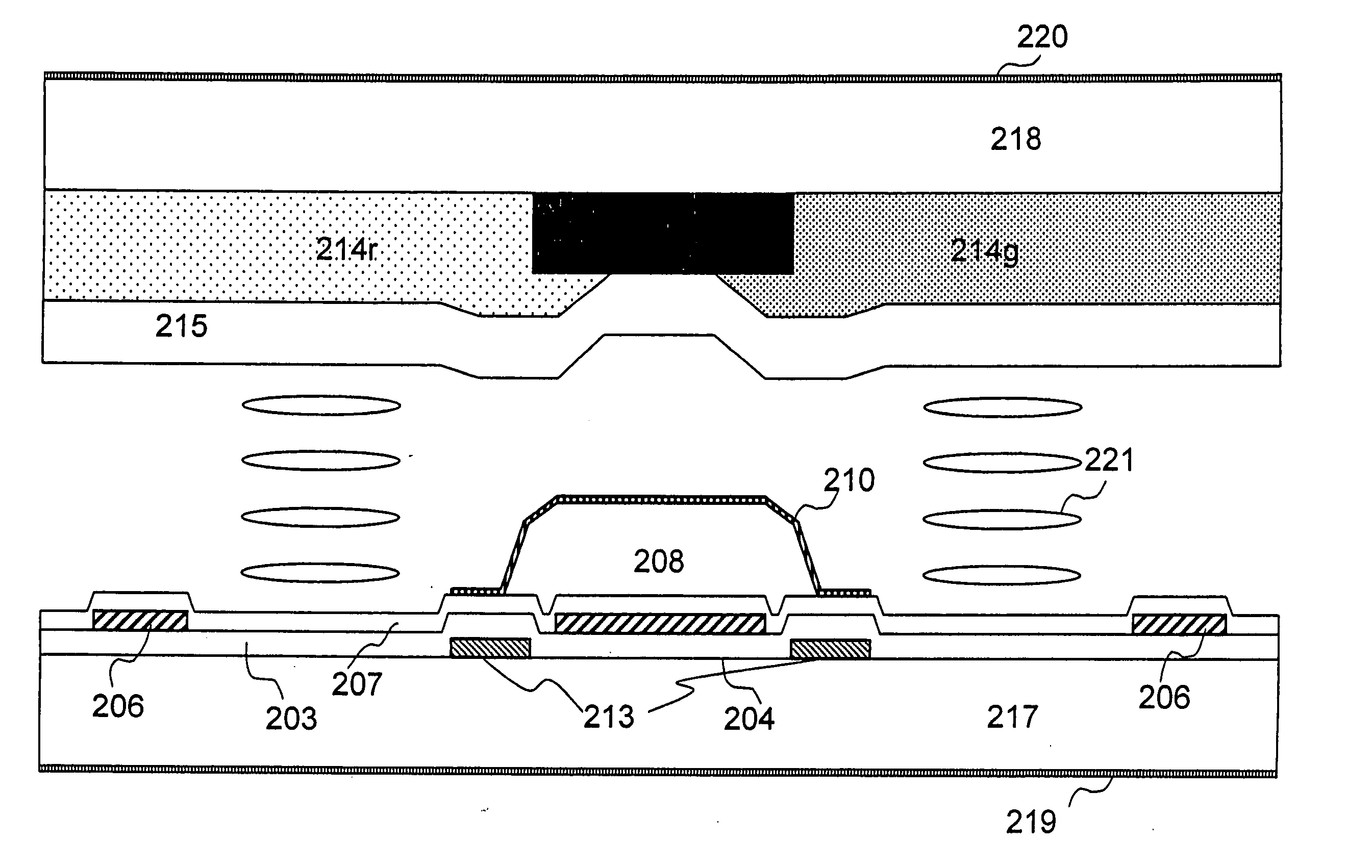
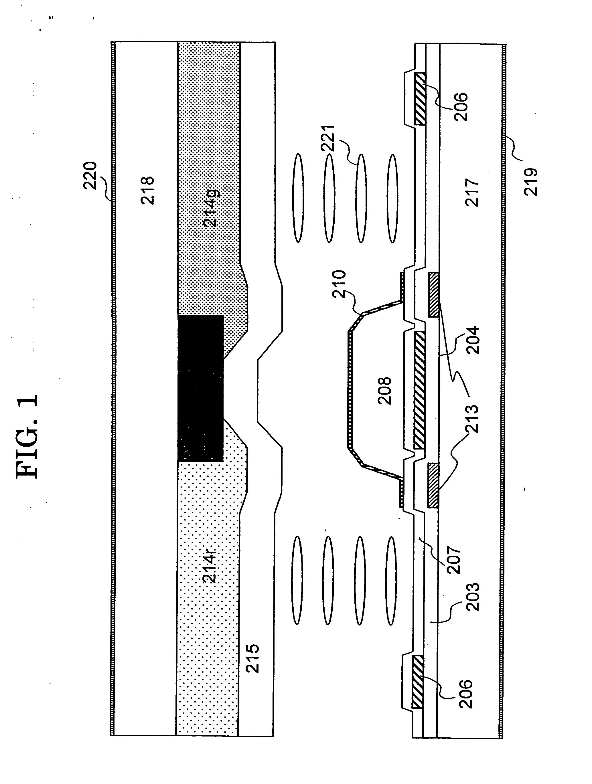
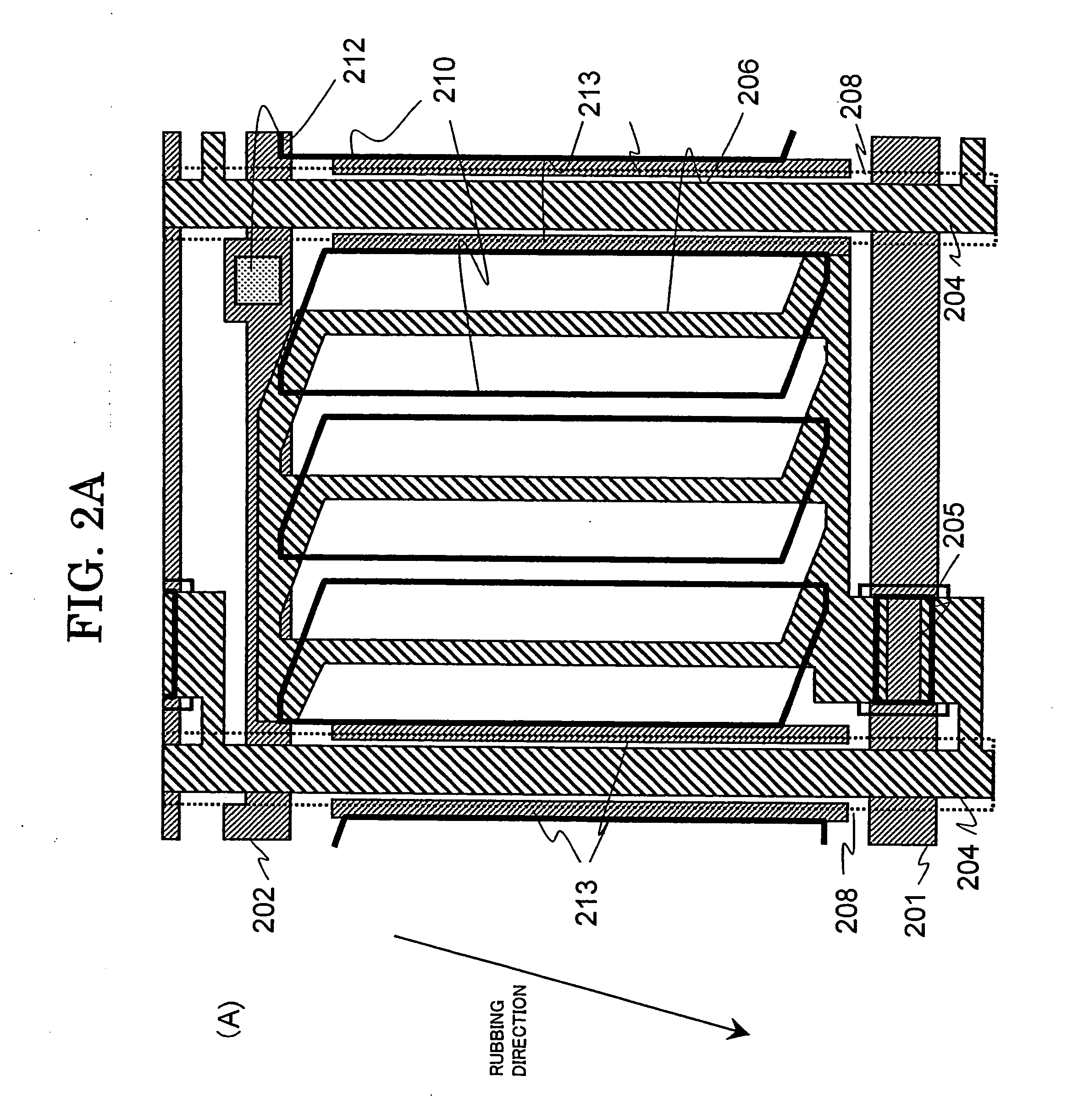
[0048]FIGS. 4A and 4B show the liquid crystal display device according to the present invention. FIG. 4A is a plan view showing one pixel, and FIG. 4B is also a plan view but with emission of a bank-like third insulating film formed on a common electrode and a video signal line in order to clarify the disposition of a light shield electrode. A scanning signal line 401 and a common signal line 402 are obtained from the same layer. Light shield electrode 413 is disposed on the rubbing inlet side of a video signal line 404. This is made so because in the case of doing the rubbing such as to stride the step, light leakage in the step part on the rubbing inlet side remains even by optimizing the rubbing conditions. The light shield electrode 413 is not connected to any other electrode, but is in the floating state.

[0049] Since light is shielded only on the light leakage occurrence side, the effective aperture factor reduction is improved compared to the double side light shielding. Also,...

fourth embodiment

[0050] the liquid crystal display device according to the present invention will now be described with reference to FIGS. 5A and 5B. FIG. 5A is a plan view showing one pixel, and FIG. 5B is also a plan view but with omission of a bank-like third insulating film formed on a common electrode and a video signal electrode in order to clarify the disposition of a light shield electrode. A scanning signal line 501 and a common signal line 502 are obtained from the same layer. A light shield electrode 513 is disposed on the rubbing inlet side of a video signal line 504. This is made so because in the case of doing the rubbing such as to stride the step, light leakage in the step part on the rubbing inlet side remains even by optimizing the rubbing condition. The light shield electrode 513 is connected to the common signal line 502 and held at the same potential.

second embodiment

[0051] Since light is shielded only on the light leakage occurrence side, the actual aperture factor reduction can be improved compared to the case of the double side light shielding. Also, although not so much as in the second embodiment, with the light shield electrode 513 connected to the common electrode, it is possible to effectively shield the electric field from the video signal line and have the effect of reducing the lateral crosstalk.


PUM


Abstract

An active matrix type liquid crystal display device in the lateral electric field system is disclosed, in which a high aperture factor is ensured even in a narrow pitch case, while also ensuring high contract and reduced vertical stroke is disclosed. In a liquid crystal display device, in which substantially bank-like third insulating film 208 is formed a video signal line 204 and covered by a common electrode 210, a light shield electrode 213 is formed underneath an extension of a common electrode 210 from an edge of a video signal line 204. With this arrangement, a liquid crystal display device is realized, which shields light from the sides of a step part as well as ensuring high aperture factor and high contrast.

Description

BACKGROUND OF THE PRESENT INVENTION [0001] This application claims benefit of Japanese Patent Application No. 2004-002782 filed on Jan. 8, 2003, the contents of which are incorporated by the reference. [0002] The present invention relates to liquid crystal display devices and, more particularly, to active matrix type liquid crystal display devices in lateral electric field system capable of obtaining high aperture factor and high contrast. [0003] The TN (twisted nematic) system which has heretofore been broadly used, ensures high contrast. On the demerit side, however, the molecular axis of liquid crystal is raised by perpendicular electric field. This means a problem of pronounced visual field angle dependency. Recently, demands for systems for large size monitors such as TV sets are increasing, and an IPS (In-Plane Switching) system has been broadly adopted. In the IPS system, for the display the molecular axis of the liquid crystal is rotated by lateral electric field in a plane ...

Claims


Application Information

Patent Timeline
IPC IPC(8): G02F1/1333G02F1/1343G02F1/136G02F1/1362G02F1/1368G11B3/58H01L29/786
CPCG02F1/134363G02F2001/136218G02F1/136209G02F1/136218A47J41/0083A47J43/07
Inventor KONNO, TAKAYUKINISHIDA, SHINICHIOKAMOTO, MAMORU
Owner NEC LCD TECH CORP
Why Eureka
Try Eureka