Circuit substrate manufacturing method

a technology of circuit substrates and manufacturing methods, applied in the direction of printed circuit board laminated, paper/cardboard articles, printed element electric connection formation, etc., can solve the problems of easy damage to the conveyer system, poor workability in handling copper plates, and cracks in carrying, so as to improve workability, prevent the generation of trouble in the conveyer system of carrying the base substrate, and improve the effect of workability

Active Publication Date: 2005-07-21
SHINKO ELECTRIC IND CO LTD
View PDF6 Cites 64 Cited by
  • Summary
  • Abstract
  • Description
  • Claims
  • Application Information

AI Technical Summary

Benefits of technology

[0018] In this manner, like the above invention, since the weight reduction of the substrate can be achieved, the workability can be improved and also generation of the trouble in carrying the base substrate by the conveyer system can be prevented. Also, in the present invention, since th

Problems solved by technology

However, according to the manufacturing methods in connection with Patent Literatures 1 to 3, since the relatively heavy copper plate is used as the substrate, various troubles are caused readily in the manufacturing steps.
Therefore, the workability in handling the copper plate is wrong and also the heavy copper plate must be carried in the manufacturing steps, and as a result the trouble is easily caused in the conveyer system.
However, if its thickness is to

Method used


Image

  • Circuit substrate manufacturing method
  • Circuit substrate manufacturing method
  • Circuit substrate manufacturing method

Examples


first embodiment

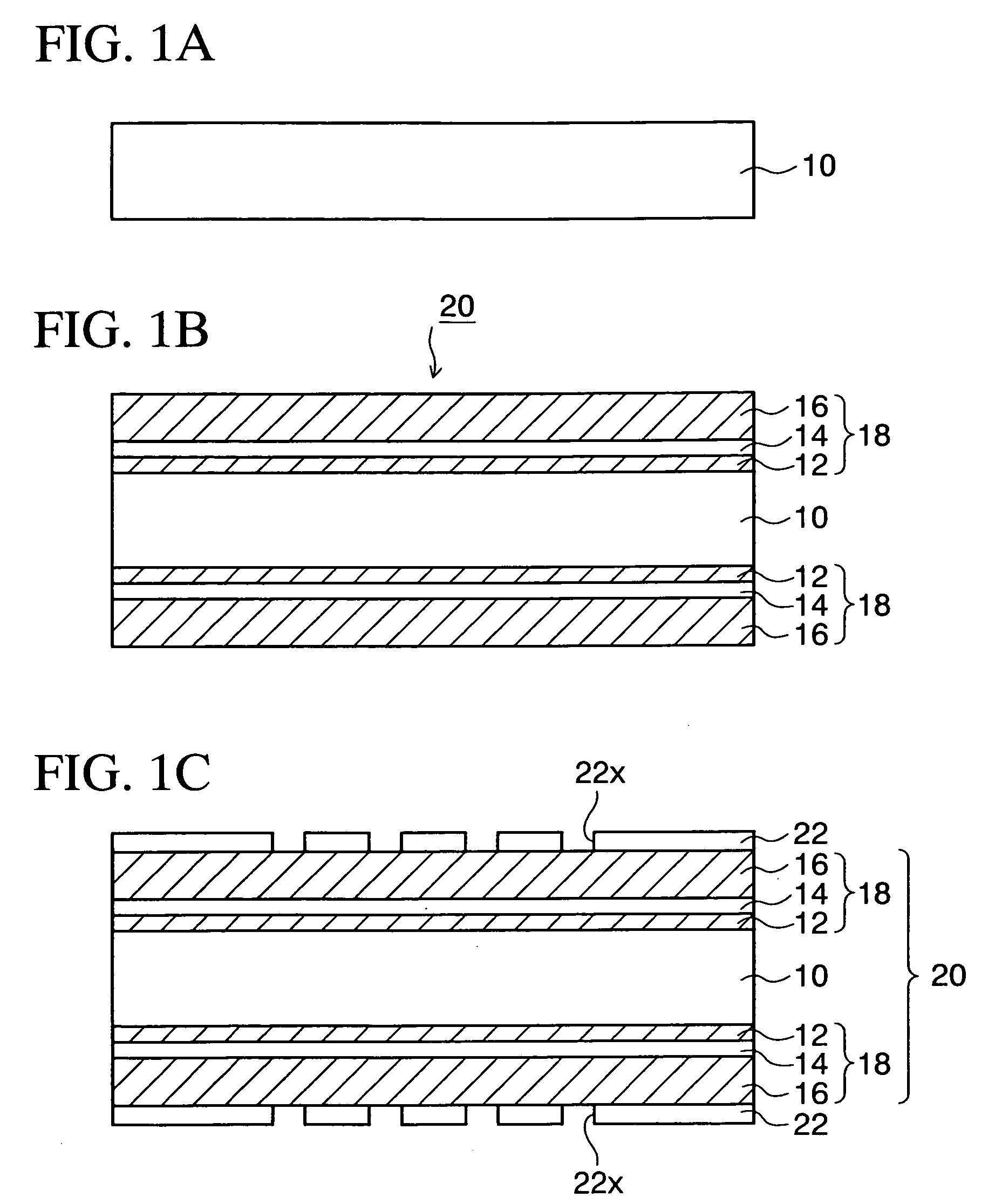
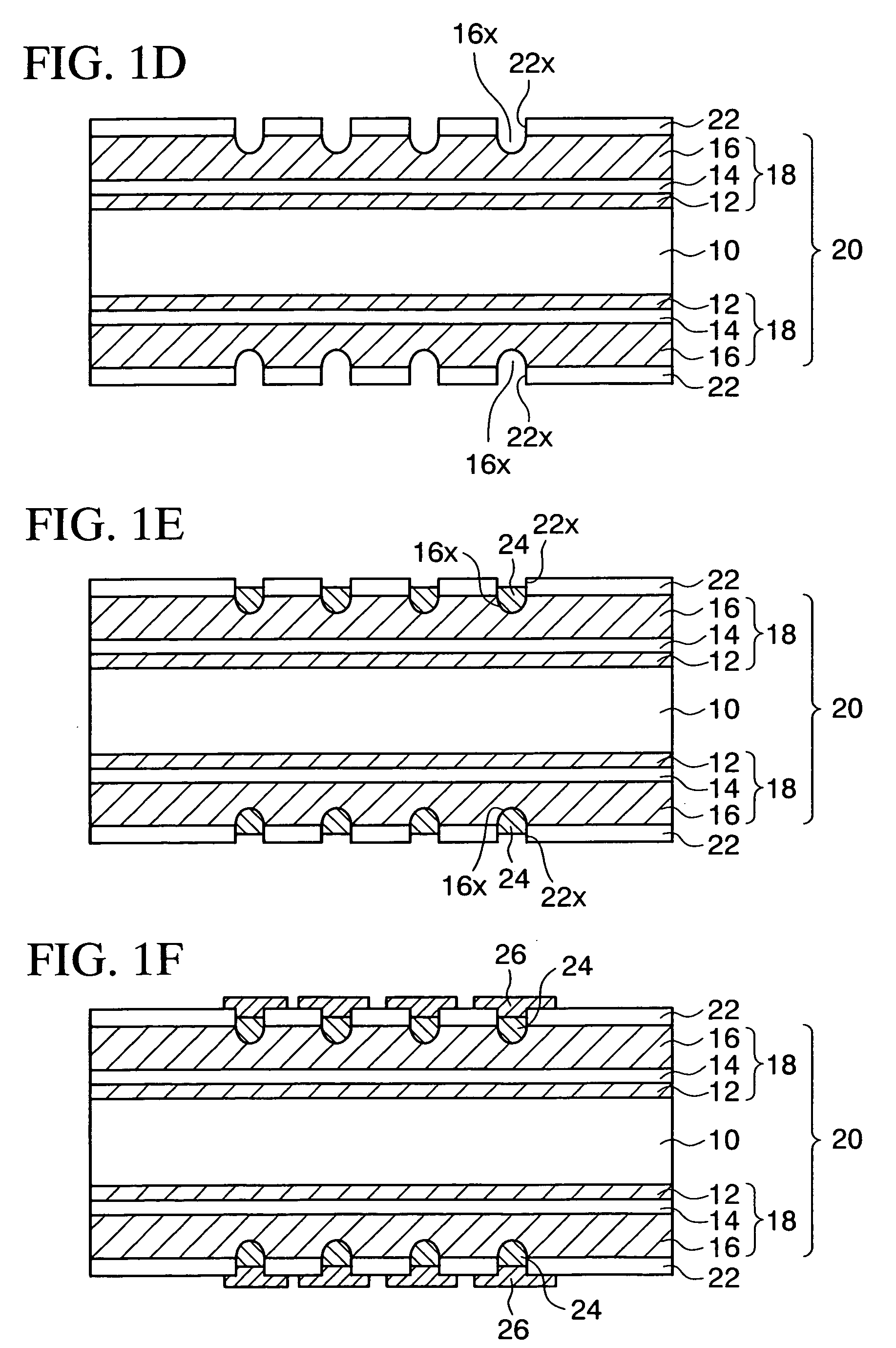
[0025]FIGS. 1A to 1L are sectional views showing a circuit substrate manufacturing method according to a first embodiment of the present invention in seriatim.

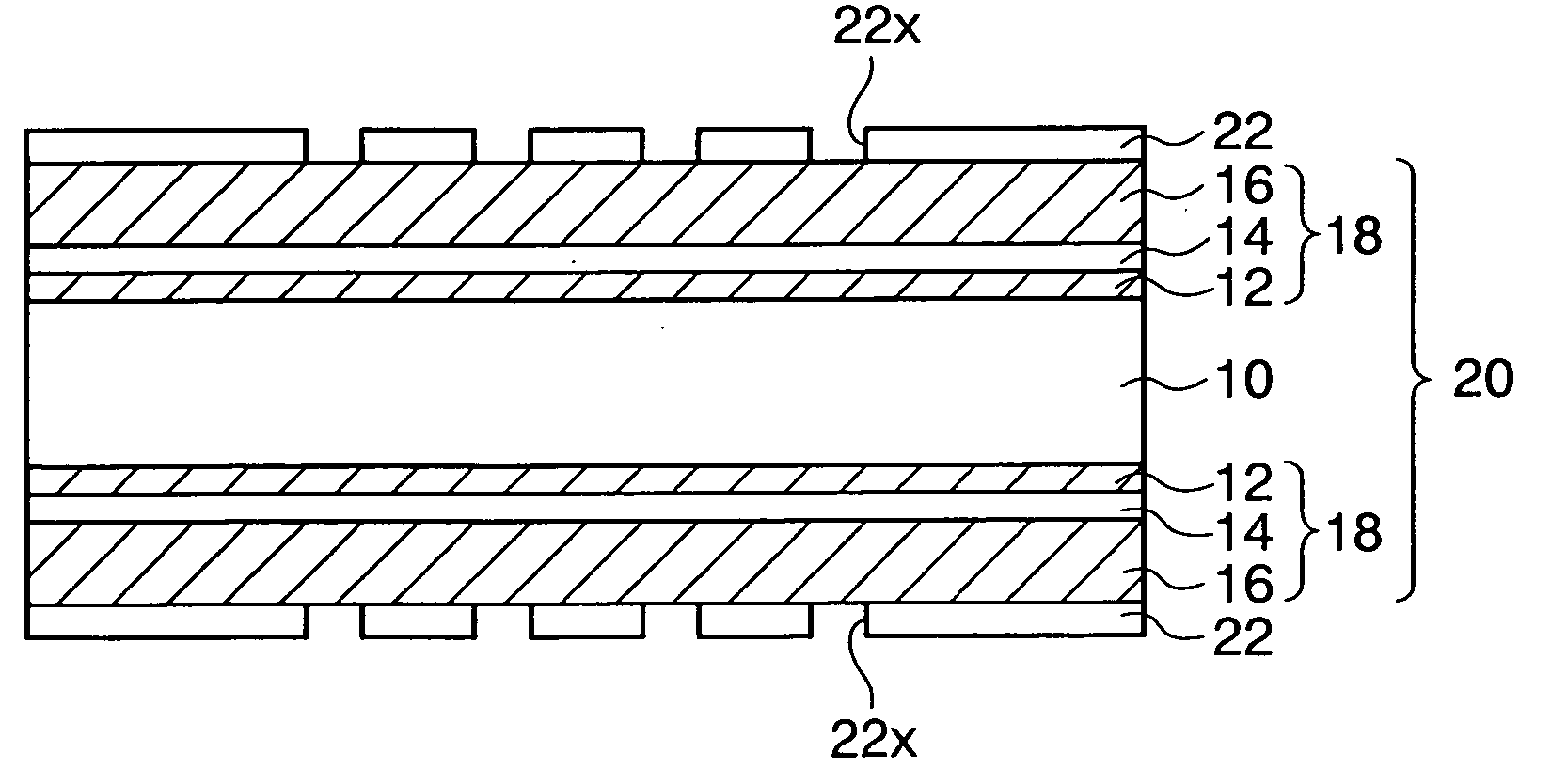
[0026] As shown in FIG. 1A, first a resin substrate 10 such as a glass epoxy resin, or the like is prepared. Then, as shown in FIG. 1B, a carrier-backed copper foil 18 having such a structure that a carrier copper foil 16 of 30 to 40 μm thickness is pasted onto a thin film copper foil 12 of 3 to 5 μm thickness via a released layer (adhesive layer) 14 is prepared. The carrier copper foil 16 is provided as a supporting member that facilitates the handling of the thin film copper foil 12.

[0027] Then, as similarly shown in FIG. 1B, an exposed surface of the thin film copper foil 12 of the carrier-backed copper foil 18 is pasted onto both surfaces of the resin substrate 10 respectively. At this time, the bump-like unevenness is provided to the exposed surface of the thin film copper foil 12 of the carrier-backed copper foil 18. T...

second embodiment

[0050]FIGS. 3A to 3I are sectional views showing a circuit substrate manufacturing method according to a second embodiment of the present invention (FIG. 3B is a plan view showing the same). A difference of the second embodiment from the first embodiment resides in that a substrate in which one copper foil layer is formed in a releasable state on the resin substrate is used as the base substrate and that the copper foil is not removed finally but the copper foil is used as the wiring pattern.

[0051] In the circuit substrate manufacturing method according to the second embodiment, as shown in FIG. 3A, first the resin substrate 10 similar to that in the first embodiment is prepared. Then, the copper foil 12 of 10 to 40 μm thickness, for example, is pasted onto both surfaces of the resin substrate 10 via an adhesive layer 13 respectively. Then, while also referring to a plan view in FIG. 3B, the adhesive layer 13 is not provided to the overall area of the resin substrate 10 but such ad...

third embodiment

[0067]FIGS. 4A to 4F are sectional views showing a circuit substrate manufacturing method according to a third embodiment of the present invention sequentially. A difference of the third embodiment from the second embodiment resides in that a substrate in which the copper foil is pasted onto the resin substrate via the released layer is used as the base substrate.

[0068] According to the circuit substrate manufacturing method according to the third embodiment, as shown in FIG. 4A, first a base substrate 20b having such a structure that the copper foil 12 is pasted onto both surface sides of the resin substrate 10 via the released layer 14 is prepared. The released layer 14 is made of silicone, or the like, and is formed such that the released layer 14 and the copper foil 12 are easily released at the boundary between them in the later step.

[0069] Then, as shown in FIG. 4B, the insulating film 32 in which the opening portions 32x are provided is formed on the copper foil 12 on both ...


PUM


Abstract

A circuit substrate manufacturing method of the present invention includes the steps of preparing a substrate on which a metallic foil made of a first metal (copper) is formed in a releasable state, forming a build-up wiring including a metal layer made of a second metal (solder) on the metallic foil, obtaining a circuit member having a structure that the build-up wiring is formed on the metallic foil by releasing the metallic foil from the substrate, and exposing the metal layer by removing selectively the metallic foil of the circuit member with respect to the metal layer.

Description

BACKGROUND OF THE INVENTION [0001] 1. Field of the Invention [0002] The present invention relates to a circuit substrate manufacturing method and, more particularly, a circuit substrate manufacturing method applicable to a package substrate of electronic parts. [0003] 2. Description of the Related Art [0004] As the method of manufacturing the circuit substrate into which electronic parts are packaged, in Patent Literature 1 (Patent Application Publication (KOKAI) 2000-323613), there is set forth the method of manufacturing the circuit substrate by forming the predetermined build-up multi-layered wiring on one surface of the copper plate, and then removing selectively the copper plate. Also, in Patent Literature 2 (Patent Application Publication (KOKAI) 2003-142617), there is set forth the method of manufacturing the circuit substrate by pasting two sheets of copper plate together via the adhesive applied to their peripheral portions, then forming the predetermined build-up multi-lay...

Claims


Application Information

Patent Timeline
IPC IPC(8): H05K1/03H05K3/46H05K1/11H05K3/00H05K3/02H05K3/06H05K3/20H05K3/34H05K3/38H05K3/40
CPCH05K1/113Y10T29/49156H05K3/0097H05K3/025H05K3/06H05K3/20H05K3/3473H05K3/386H05K3/4007H05K3/4682H05K2201/09563H05K2201/09909H05K2203/0152H05K2203/0156H05K2203/0338H05K2203/0376H05K2203/0726H05K2203/0733H05K2203/1536Y10T29/49155Y10T29/49128Y10T29/49126H05K3/0058H05K3/46
Inventor NAKAMURA, JUNICHI
Owner SHINKO ELECTRIC IND CO LTD
Why Eureka
Try Eureka